Showing posts with label converter. Show all posts

Saturday, November 8, 2014

12 V Glow Plug Converter

Most small internal-combustion engines commonly used in the model-building world use glow plugs for starting. Unfortunately, glow plugs have an operating voltage of 1.5 V, while fuel pumps, starter motors, chargers and the like generally run on 12 V. This means that a separate battery is always needed to power the glow plug. The standard solution is to use an additional 2-V lead storage battery, with a power diode in series to reduce the voltage by approximately 0.5 V. However, this has the annoying consequence that more than 30 percent of the energy is dissipated in the diode. Naturally, this is far from being efficient. 

Circuit diagram :

12-V Glow Plug Converter Circuit Diagram
The converter presented here allows glow plugs to be powered from the 12-V storage battery that is usually used for fuelling, charging, starting and so on. A car battery can also be used as a power source. Furthermore, this circuit is con-siderably more efficient than the approach of using a 2-V battery with a series power diode. 

The heart of the DC/DC converter is IC1, a MAX 1627. The converter works according to the well-known step-down principle, using a coil and an electrolytic capacitor. Here the switching stage is not integrated into the IC, so we are free to select a FET according to the desired current level. In this case, we have selected a 2SJ349 (T1), but any other type of logic-level FET with a low value of RDSonwould also be satisfactory. Of course, the FET must be able to handle the required high currents. 

Diode D1 is a fast Schottky diode, which must be rated to handle the charging currents for C2 and C3. This diode must also be a fairly hefty type. The internal resistances of coil L1 and capacitors C2 and C3 must be as low as possible. This ensures efficient conversion and prevents the components from becoming too warm.
The resistor network R2/R3 causes 87 percent of the output voltage to be applied to the FB pin of IC1. This means that an output voltage of 1.5 V will cause a voltage of approximately 1.3 V to be present at the FB pin. The IC always tries to drive the switching stage such that it ‘sees’ a voltage of 1.3 V on the FB input. If desired, a different output voltage can be provided by modifying the values of R2 and R3. 

When assembling the circuit, ensure that C5 and C1 are placed as close as possible to IC1, and use sufficiently heavy wiring between the 12-V input and the 1-5-V output, since large cur-rents flow in this part of the circuit
Here continue read..

Thursday, September 25, 2014

True RMS Converter Circuit

An absolute value circuit, using the CA313O is shown. During positive excursions, the input signal is fed through the feedback network directly to the output.
Simultaneously, the positive excursion of the input signal also drives the output terminal (No. 6) of the inverting amplifier negative such that the 1N914 diode effectively disconnects the amplifier from the signal path. During the negative going excursion of the input signal, the CA313O functions as a normal inverting amplifier with a gain equal to R2/R1. When the equality of the two equations shown is satisfied, the full-wave output is symmetrical. 

Peak-detector circuits are easily implemented with the CA3130, as illust- rated. lt should be noted that with large-signal inputs, the bandwidth of the peak-negative circuit is much less than that of the peak-positive circuit. The second stage of the CA313O limits the bandwidth in this case. 


Here continue read..

Friday, September 5, 2014

Basic Sine wave Converter Wiring diagram Schematic

This is a simple Basic Sine wave Converter Circuit Diagram. The schema can be used as the signal source of calibration level meter or sensor-driven differential transformer. Circuit oscillation frequency is determined by the 74HCO4, and it is transferred lkHz by R. The supply voltage of Tl changes with the amplitude output. The switch turns the output voltage into square wave, then it will get sine wave by filtering the high frequency by low-pass filter. Waveform distortion depends on the performance of the filter, and the series of filter is used according to the need. 

Basic Sine wave Converter Circuit Diagram


Basic

Here continue read..

Wednesday, December 25, 2013

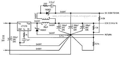
3 3V And 5V Outputs Dc Dc Converter Circuit Diagram

This is the 3.3V And 5V Outputs - Dc-Dc Converter Circuit Diagram. This Input, voltages can range from 8 V to 30 V. The load range on the 5 V is 0,05 A to 5 A while the 3.3-V load range is 0.1 A to 1 A. The circuit is self-protected under no-load conditions. Over all load and line conditions, .including cross regulation, the 3.3-V output varies from 3.25 V to 3.27 V. The 5-V output varies from 4.81 V to 5.19 V under the same conditions. 

In a typical application to 0.5 A on the 3.3 V and 0.25 A on the 5 V, efficiency is typically 76%, With an input voltage of 30 V and a full-load condition, the efficiency drops to 66%. In normal operating regions, efficiency is always better than 70%.The 5-V ripple is less than 75 mV and the 3.3-V ripple less than 50 mV over all line and load conditions.

3.3V And 5V Outputs - Dc-Dc Converter Circuit Diagram

3.3V And 5V Outputs - Dc-Dc Converter Circuit Diagram

Here continue read..

Tuesday, December 24, 2013

12Volt to 9Volt DC Converter

To get a more precise output voltage, replace zener diode Z1 with 10V and R1 with a 1Kilo ohm potentiometer. A Coolrib for Q1 is optional but highly recommended. You can replace Q1 for a more robust type to get more output amps depending on your requirements. Simple circuit to power your 9 volt cassette recorder and other stuff.


Parts List:
R1 = 560 ohm
C1 = 1000uF/40V, Electrolytic
C2 = 10uF/25V, Electrolytic
C3 = 330nF, Ceramic
Z1 = 9.1V, 1watt zener
Q1 = ECG184, NTE184
Here continue read..