Showing posts with label circuit. Show all posts

Thursday, November 20, 2014

Ultra Fast Battery charger circuit

Ultra Fast Battery Chager for Nickel-Cadmium battery cells [NiCad] which will be discussed in this article is Fast NiCad Battery Charger, called the Ultra Fast Charger Battery Charger NiCad because it can make filling fast NiCad Batteries Cell. A battery charger in Desai has a fast charging capabilities such as Ultra Fast Battery Chager for Nickel-Cadmium battery cells [NiCad] on this article shall be equipped with some ability to protect the battery and charger circuit itself.

Feature owned by Ultra Fast Battery Chager for Nickel-Cadmium battery cells [NiCad] 

  • Autoshut-off, is the ability of the charger to stop charging current to a NiCad battery if the capacity NiCad battery is fully charged.
  • Polarity Protection, with the existence of this capability so if there are mounting the battery on the charger upside yan can be known.
  • Constant output voltage
  • Output currents enough to fill some NiCad batteries at once in parallel.
  • Short Circuit Protection, with the existence of this protection circuit so if there is short-circuit caused by a battery and a charger circuit itself will not damage the other parts are not damaged.
  • Series Ultra Fast Battery Chager for Nickel-Cadmium battery cells [NiCad]


Image series above is a series of schematic drawings for Ultra Fast Battery Chager for Nickel-Cadmium battery cells [NiCad]. Ultra Fast Battery Chager for Nickel-Cadmium battery cells [NiCad] can be used for 8 to 10 NiCad batteries at once with 12 volt output voltage and max current is 3.5 A. The main components in the circuit of Ultra Fast Battery Chager for Nickel-Cadmium battery cells [NiCad] is UC3843 and MC34181. UC3843 chip is a voltage regulator and M34181 is a JFET OpAmp with characteristic low offset voltage, input impedance is very high. MC34181 serves as a voltage comparator.
Here continue read..

Easy Downloader Circuit

Atmel microcontroller series AT89Cxx51 Easy Downloader is one of the downloader that is often used to write data to program the Atmel microcontroller AT89CXX51. Easy Downloader AT89Cxx51 ATMEL microcontroller is using the serial port as a channel of communication with the computer. Easy Downloader ATMEL Microcontroller AT89Cxx51 can be used to program Atmel AT89CXX51 in parallel. Atmel microcontroller series AT89Cxx51 Easy Downloader is quite simple to make your own because the components necessary to membutanya not complex. Atmel microcontroller series AT89Cxx51 Easy Downloader do not support the serial programming microcontrollers ISP. In the article Easy Downloader ATMEL Microcontroller AT89Cxx51 only displays images Easy Downloader Microcontroller series from Atmel AT89Cxx51 mengulasnya only and are simple.


Here continue read..

Wednesday, November 19, 2014

144 MHz Simple RF Detector Circuit


This simple circuit helps you sniff out RF radiation from your transmitter, improper joints, a broken wire or poor equipment with RF shielding. The tester is designed for the radio band amateur 2 meter (144-146 MHz in Europe). The instrument has a reading of 4-step LED and an audible alarm for high voltage radiation. The RF signal is received by an antenna and made to resonate by C1-L1. After rectification by the diode D1, the signal is fed to a two transistor Darlington amplifier HighGain, T2-T3. Assuming a 10-inch telescoping antenna using the RF level scale established for the LEDs is as follows:

When all the LEDs light, the (optional) UM66 sound / melody generator chip (IC1) also operates and provides an audible alarm. By changing the zener diode values ​​of D2, D4, D6 and D8, the step size and duration of the instrument may change as needed. To operate in other bands of ham or PMR, simply change the network-L1 C1 resonance.

For example, a transceiver 5 watt handheld equipped with a telescoping half-wave antenna (G = 3.5 dBd), there is an ERP (Effective Radiated Power) of just 10 watts and an emf of more than 8 volts near the head. Inductor L1 consists of 2.5 turns of 20 SWG (approximately 1 mm in diameter) enameled copper wire. The inner diameter is approximately 7 mm and no core is used.

Trimmer capacitor C1 associates is adjusted for the greatest number of LEDs to light at a relatively low fieldstrength position for a 2 m transceiver 145 MHz transmission. The tester is powered by a 9 V battery and consumes about 15 mA when all LEDs are on. Must be enclosed in a metal box.
Here continue read..

Tuesday, November 18, 2014

230Volt LED Circuit

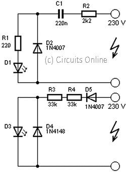
This is a circuit that is used to menhidupkan LED with voltage 230Volt, 230Volt it so that the voltage must be lowered in accordance with the needs of the LED itself. To lower it even necessary circuit as below.

230Volt

Here continue read..

Loop Control Automatic Reversing Circuit Diagram

LoopLoop Control Automatic Reversing Circuit Diagram

It is not the purpose of this folio to accommodate a abundant account of the ICs acclimated by this circuit. If you appetite added advice on this accountable amuse accredit to the Flip-Flop Made With A LM556 Timer Chip folio in the assorted circuits area of this armpit and additionally the Visible Light Photo Detector Circuits.

*The ambit uses the basal phototransistor detector ambit to faculty the position of a alternation that is abutting or is in the abandoning loop.

*Track polarity abandoning is not covered by this folio and will accept to be bent by the user.

Please Read Afore Using These Ambit Ideas

The explanations for the circuits on these pages cannot achievement to awning every bearings on every layout. For this acumen be able to do some experimenting to get the after-effects you want. This is abnormally accurate of circuits such as the "Across Track Infrared Detection" circuits and any added ambit that relies on added than absolute cyberbanking inputs, such as switches.

If you use any of these ambit ideas, ask your genitalia supplier for a archetype of the manufacturers abstracts bedding for any apparatus that you accept not acclimated before. These bedding accommodate a abundance of abstracts and ambit architecture advice that no cyberbanking or book commodity could access and will save time and conceivably accident to the apparatus themselves. These abstracts bedding can generally be begin on the web armpit of the accessory manufacturers.

Although the circuits are anatomic the pages are not meant to be abounding descriptions of anniversary ambit but rather as guides for adapting them for use by others. If you accept any questions or comments amuse accelerate them to the email abode on the Ambit Index page.

Here continue read..

Monday, November 17, 2014

GSM Cell Phone Jammer Circuit

GSMGSM Cell Phone Jammer Circuit

A admirable diy gsm jammer or cellular adaptable buzz jammer schematic diagram for use alone in GSM1900 with abundance from 1930 MHz to 1990 MHz. The GSM1900 cellular corpuscle buzz arrangement is fabricated use of by USA, Canada and best of the nations in South America.

This cellular buzz jammer isnt applicative for use in Europe, Center East, nor Asia. The GSM jammer ambit could block adaptable adaptable buzz signals which operates on GSM1900 band, additionally articular as DCS.
Here continue read..

Sunday, November 16, 2014

Kawasaki ZRX1200 Radiator Fan Circuit Diagram

KawasakiKawasaki ZRX1200 Radiator Fan Circuit Diagram

To inspect and service the 2001 to 2006 Kawasaki ZRX1200 R/S radiator fan system, do the following:

* Remove fuel tank.
* Disconnect the 2 pin connector from radiator fan switch.
* Using an auxiliary wire, connect the radiator fan switch leads of the main harness side.
* Turn the ignition switch ON. If the fan rotates, inspect the fan switch. If the fan does not rotate, inspect: leads and connectors, main fuse, fan fuse, and fan motor.
 
1. Radiator Fan
2. Radiator Fan Switch
3. Junction Box
4. Fan Fuse 10A
5. Main Fuse 30A
6. Battery 12V14Ah
Here continue read..

Friday, November 14, 2014

INVERTER CIRCUIT 100 WATT

Inverter is a small circuit which will convert the direct current (DC) to alternating current (AC). The power of a battery is converted in to’ main voltages’ or AC power. This power can be used for electronic appliances like television, mobile phones, computer etc. the main function of the inverter is to convert DC to AC and step-up transformer is used to create main voltages from resulting AC.

Block Diagram of Inverter


In the block diagram battery supply is given to the MOSFET driver where it will convert DC to AC and the resulting AC is given to the step up transformer from the step up transformer we will the get the original voltage.

Main Components

CD4047 : CD4047 is a multi vibrator with very low power consumption designed by TEXAS INSTRUMENTS.it can operate in monostable multivibrator and also astable multivibrator.in the astable multivibrator mode it can operate in free running or gatable modes and also provides good astable frequency stability. It can generate 50% duty cycle which will create a pulse, which can be applied for inverter circuit. This is mainly used in frequency discriminators, timing circuits frequency divisions etc.

IRF540 : IRF540 is a N-channel enhanced mode silicon gate field effect transistor (MOSFET).they are mainly used in switching regulators, switching converters relay drivers etc. the reason for using them in the INVERTER circuit is the because it is a high switching transistor , can work in very low gate drive power and have high input impedance.

IRF540 Symbol


Circuit Diagram


Explanation

  • In the circuit diagram we can observe that 12V battery is connecter to the diode LED and also connected to the pin8 of the IC 4047 which is VCC or power supply pin and also to pin 4 and 5 which are astable and  complement astable of  the IC. Diode in the circuit will help not give any reverse current, LED will work as a indicator to the battery is working or not.
  • IC CD4047 will work in the astable multivibrator mode. To work it in astable multivibrator mode we need an external capacitor which should be connected between the pin1 and pin3. Pin2 is connected by the resistor and a variable resistor to change the change the output frequency of the IC. Remaining pins are grounded .The pins 10 and 11 are connected to the gate of the mosfets IRF540. The pin 10 and 11 are Q and ~Q from these pins the output frequencies is generated with 50% duty cycle.
  • The output frequency is connected to the mosfets through resistor which will help to prevent to the loading of the mosfets. The main AC current is generated by the two mosfets which will act as a two electronic switches. The battery current is made to flow upper half or positive half of the primary coil of transformer through Q1 this is done when the pin 10 becomes high and lower half or negative half is done by opposite current flow through the primary coil of transformer, this is done when pin 11 is high. By switching the two mosfets current is generated.
  • This AC is given to the step up transformer of the secondary coil from this coil only we will get the increased AC voltage , this AC voltage is so high; from step up transformer we will get the max voltage. Zenor diode will help avoid the reverse current.

NOTE : The generated AC is not equal to the normal AC mains or house hold current. You cannot use this voltage for pure electric appliances like heater, electric cooker etc. Because of the fast switching of mosfets heat is dissipated which will effect the efficiency, use heat sink to remove this problem.
Here continue read..

Wednesday, November 12, 2014

indicator alarm for Water level circuit with explanation


This electronic circuit is a simple water level indicator alarm that is based on few transistors . The circuit is very simple and it has a very low current consumption , so you can use a 9 volts battery to powering this water level indicator alarm . This water level indicator alarm electronic circuit can be used even for rain alarm or short circuit alarm , a resistance with a value from 0 to about 1 M ohm will trigger it . The Q1 transistor acts as a switch which applies current to the unijunction relaxation oscillator Q2 . The signal frequency of the alarm circuit is give by the values and ratios of the C1 / R2 .

If you don’t have the transistors marked on the schematic diagram you can replace them almost with any similar types . As you can see in the schematic diagram , between probes is mounted a switch ( you can use a push-button) for testing the circuit , but it can be removed .
The speaker used in this project must have a impedance between 15 and 90 ohms .
Here continue read..

LM317 based DC motor speed controller with circuit


A very simple DC motor speed controller circuit can be constructed using a LM317 voltage regulator integrated circuit . This DC motor speed controller can be used for speed control of mini drills or for other small DC motors . This motor controller circuit will provide a large output current . The maximum output current from the secondary turns of the transformer shout provide 1.5 times of the maximum DC output current . The output voltage and the speed ( rpm ) is set by the P2 variable resistor .

As soon as the current drawn exceeds a certain value , T2 will be switched on . This results in a base current for T3 so that R5 is in parallel with R6 . This automatically raise the output voltage to counter a threatened drop in rpm . The moment at which this action occurs is set by P1 .

Here continue read..

Suzuki GSX400F’82 Signal Generator Circuit Diagram

Suzuki

The 1982 Suzuki GSX400F signal generator is mounted on the right hand side of the engine in the area commonly used for contact breaker point. It is comprised of a magnet embedded rotor attached to a mechanical advance mechanism and two pick-up coils, with iron plates at their bases, affixed to a plate. Each pick-up coil consists of a coil of wire and a yoke or coil and is mounted, 180 degree apart on the plate. As the rotor magnet is turned past the coils, AC current is produced and used for switching within the transistor unit. The transistor unit controls power to the ignition coils and causes the spark plugs to fire at the proper time.

Here continue read..

Sunday, November 2, 2014

VW CAR PASSAT ENGINE ELECTRICAL WIRING CIRCUIT


VW CAR PASSAT ENGINE ELECTRICAL WIRING CIRCUIT

VW Passat wiring diagram are shown in the following figure. It shows the connection and wiring between each parts and component of engine compartment and headlights system of the vehicle such as the anti theft control unit, fuse/relay panel, headlight, battery, starter, alternator, starter interlock relay, warning indicators, cruise control switch, horns, clutch pedal switch, vacuum pump motor, cruise control unit, radiator cooling fan thermo switch, radiator cooling fan control unit, radiator fan motor, third speed coolant fan thermo switch, after run cooling fan thermo switch, and many more.
Here continue read..

10 W Audio Amplifier Circuit

This circuit is a general-purpose 10-W audio amplifier for moderate-power PA or modulator use in an AM transmitter. With higher voltages and a change in bias resistors, up to 30 W can be obtained. The Output Stage Amplifier using transistor 2N3055 and MJE2055.

10 W Audio Amplifier Circuit Diagram
Here continue read..

Saturday, November 1, 2014

2 Way Speaker Crossover circuit

The series of crossover is an electronic circuit in which the point to separate the audio sound frequency. objective that only sound with a frequency range that can be accepted speakers are forwarded. less is more like a filter function, so the speakers work optimally.

2 way or 3 way or else, that determines how many channels would be separated voice. Each channel is handled by a single class of speakers. Eg 3 way, the frequency of sound produced by the head unit, separated by crossover as a low freq (big size distinguished speaker better known as the subwoofer), medium freq (medium speakers), usually in the middle) and hi freq (small speakers I would call a tweeter) Let me better sound and reduce noise.

Schematic 2 Way Speaker Crossover
Here continue read..

Friday, October 31, 2014

Digital Step Km Counter Circuit Diagram

This circuit measures the distance covered during a walk. Hardware is located in a small box slipped in pants pocket and the display is conceived in the following manner: the leftmost display D2 (the most significant digit) shows 0 to 9 Km. and its dot is always on to separate Km. from hm. The rightmost display D1 (the least significant digit) shows hundreds meters and its dot illuminates after every 50 meters of walking. A beeper (excludable), signals each count unit, occurring every two steps. A normal step was calculated to span around 78 centimeters, thus the LED signaling 50 meters illuminates after 64 steps (or 32 operations of the mercury switch), the display indicates 100 meters after 128 steps and so on.

For low battery consumption the display illuminates only on request, pushing on P2. Accidental reset of the counters is avoided because to reset the circuit both pushbuttons must be operated together. Obviously, this is not a precision meter, but its approximation degree was found good for this kind of device. In any case, the most critical thing to do is the correct placement of the mercury switch inside of the box and the setting of its sloping degree.

Digital Step-Km Counter Circuit diagram:


digital_step_km_counter_circuit_diagram
Digital Step-Km Counter Circuit Diagram


Parts:
R1 = 22K 1/4W Resistor
R2 = 2.2M 1/4W Resistor
R3 = 22K 1/4W Resistor
R4 = 1M 1/4W Resistor
R5 = 4.7K 1/4W Resistor
R6 = 47R 1/4W Resistor
R7 = 4.7K 1/4W Resistor
R8 = 4.7K 1/4W Resistor
R9 = 1K 1/4W Resistor
C1 = 47nF 63V Polyester Capacitor
C2 = 100nF 63V Polyester Capacitor
C3 = 10nF 63V Polyester Capacitor
C4 = 10µF 25V Electrolytic Capacitor
D1 = Common-cathode 7-segment LED mini-display (Hundreds meters)
D2 = Common-cathode 7-segment LED mini-display (Kilometers)
Q1 = BC327 45V 800mA PNP Transistors
Q2 = BC327 45V 800mA PNP Transistors
P1 = SPST Pushbutton (Reset)
P2 = SPST Pushbutton (Display)
IC1 = 4093 Quad 2 input Schmitt NAND Gate IC
IC2 = 4024 7 stage ripple counter IC
IC3 = 4026 Decade counter with decoded 7-segment display outputs IC
IC4 = 4026 Decade counter with decoded 7-segment display outputs IC
SW1 = SPST Mercury Switch, called also Tilt Switch
SW2 = SPST Slider Switch (Sound on-off)
SW3 = SPST Slider Switch (Power on-off)
BZ = Piezo sounder
B1 = 3V Battery (2 AA 1.5V Cells in series)

Circuit operation:

IC 1A & IC 1B form a monostable multi vibrator providing some degree of freedom from excessive bouncing of the mercury switch. Therefore a clean square pulse enters IC2 that divides by 64. Q2 drives the LED dot-segment of D1 every 32 pulses counted by IC2. Either IC3 & IC4 divide by 10 and drive the displays. P1 resets the counters and P2 enables the displays. IC1C generates an audio frequency square wave that is enabled for a short time at each monostable count. Q1 drives the piezo sounder and SW2 allows disabling the beep.

Notes:
  • Experiment with placement and sloping degree of mercury switch inside the box: this is very critical.
  • Try to obtain a pulse every two walking steps. Listening to the beeper is extremely useful during setup.
  • Trim R6 value to change beeper sound power.
  • Push P1 and P2 to reset.
  • This circuit is primarily intended for walking purposes. For jogging, further great care must be used with mercury switch placement to avoid undesired counts.
  • When the display is disabled current consumption is negligible, therefore SW3 can be omitted.
Here continue read..

Tri Waveform Generator Circuit Diagram

This is the simple Tri-Waveform Generator Circuit Diagram. The Tri-Waveform Generator can be used for a number of different uses. The one that I use it for is a signal generator to test circuits. The frequency range is 20 to 20khz. and can be adjusted by R1. The duty cycle or the time that the waveform is high and the time that the waveform is low can be adjusted by R4. The purpose of R2 and R3 are to clean up any distortion on the sine wave output. To do this you must hook up the sine wave output to and oscilloscope and adjust R2 & R3 to make the sine wave as accurate as possible.

Here continue read..

Thursday, October 30, 2014

Electric Stable USB Power Supply Circuit Diagram

This is an Electric Stable USB Power Supply Circuit Diagram. A common problem when an AC mains adapter is used to power a USB device is that the voltage does not match the nominal 5 V specified by the USB standard. The circuit shown here accepts an input voltage in the range of 4-9 V and converts it into a 6-V output voltage, which is then stabilized to a clean 5-V level by a series regulator. The combined boost/buck converter used here operates on the SEPIC principle. That principle is quite similar to the operating principle of the Cuk converter, but without the disadvantage of a negative output voltage.

Stable USB Power Supply Circuit diagram :

Stable-USB-Power-Supply-Circuit-Diagram

Stable USB Power Supply Circuit Diagram

The circuit is built around a MAX668, which is intended to be used as a controller for boost converters. The difference between a SEPIC converter and a standard boost (step-up) converter is that the former type has an additional capacitor (in this case C2) and a second inductor (in this case, the secondary winding of transformer L1). If C2 is replaced by a wire bridge and the secondary winding of L1 is left open, the result is a normal boost converter. In that case, a current can always flow from the input to the output via L1 and D1, even when the FET is not driven by IC1. Under these conditions, the output voltage can never be less than the input voltage less the voltage drop across the diode.

The operation of a SEPIC converter can be explained in simple terms by saying that C2 prevents any DC voltage on the input from appearing at the output, so the output voltage can easily be made lower than the input voltage. The second coil causes a defined voltage to be present at the anode of D1. It is also possible to replace the transformer by two separate coils that are not magnetically coupled. However, the efficiency of the circuit is somewhat higher if coupled coils are used as shown here. The value of resistor R4 is chosen to limit the maximum current to 500mA, which is also the maximum current that a USB bus can provide according to the specifications. Resistors R1 and R2 cause the voltage across C3 and C7 to be regulated at a value of around 6 V. A low-drop regulator (LM2940) is used to generate a stabilized 5V from the 6V output (with ripple voltage). The efficiency should be somewhere between 60% and 80%
Here continue read..

Wednesday, October 29, 2014

Advance High Voltage Stun Gun Circuit Diagram


This is an Advance High Voltage Stun Gun Circuit Diagram, This device produces high voltage pulses discrupting muscles and nervous sYstem, leaving anyone who touches it in a state of menthal confusion. Can be used agains ferocious animals or attackers, BUT REMEMBER, this device may be illegal in your state (for eg where I live, these devices are banned). It is quite dangerous for peoples experiencing cardiac problems, and for electronic equipment (like peacemakers), since it generates some RF. Dont attept irresponsible actions with this device, it is not a toy.

 Advance High Voltage Stun Gun Circuit Diagram


Advance


After the introduction lets pass to the circuit.

The 555 IC is wired as a astable to produce square wave with adjustable freq and duty cycle (notice the potentiometers and diode). This square wave is feed to a IRF840 Mosfet (no need of totem transistors since freq is low and the IC has enough current capability to rapidly charge/discharge the gate). As a substitute of the mosfet, a bipolar transistor can be used (and a 100ohm resistor between 555 and base of the transistor). Valid BJT can be BU406, but also smaller BJT can be ok, keep in mind that it must handle at least 2A continuous. The inductive kick snubber isnt needed because the power is low and it is almost totally adsorbed to charge the tank capacitor, in addition since this device is battery operated we dont want to dissipate the power on a resistor but we want it in sparks. With a snubbing network you will experience lower firing rates. 
USE A PUSHBUTTON SWITCH FOR SAFETY
Construction of T2: this is the real boring part. Since it is unlikely to find it in shops we need to build them. Materials needed: enamel copper wire (0,20 mm or 0,125 mm), ferrite stick, LDPE sheets (0,25 mm). Secure the ferrite stick with a layer of ldpe (polyethilene, as a substiture use electric insulating tape) and glue it (or tape it) Place 200-250 windings on the ldpe (even more windings if the stick is more than 1), another ldpe layer, another 200-250 windings and so on to finally have 5-6 layers (approx 1000-1400 turns but even more doesnt hurt performance, but be careful for internar arcing that will ruin it). Insulate it again and place the primary winding, 15-20 turns of 1mm wire are just ok, too much windings (too mush resistance and inductance) will lead to smaller current and smaller spike in T2 secondary because of lower rise time,and too few will not saturate the core. I chosen MKP capacitors because they have low ESR and ESL (they are widely used in tesla coils as mmc capacitors).

The spark gap can be simple two crossed (but not touching) 1 mm spaced wires. It acts as a voltage controlled switch, firing when the voltage is enough to ionize the air between them (turning it to plasma with small resistance). Keep in mind that it would be wise do place it into a small plastic container and fill with oil letting bubbles out (dont use motor oir or frying oil but pure mineral oil which has no water in it.

Author:Jonathan Filippi, jonathan.filippi@virgilio.it
Here continue read..

Mic Audio Amplifier Circuit Diagram

The compact, low-cost condenser mic audio amplifier described here provides good-quality audio of 0.5 watts at 4.5 volts. It can be used as part of intercoms, walkie-talkies, low-power transmitters, and packet radio receivers. Transistors T1 and T2 form the mic preamplifier. 

Resistor R1 provides the necessary bias for the condenser mic while preset VR1 functions as gain control for varying its gain. In order to increase the audio power, the low-level audio output from the preamplifier stage is coupled via coupling capacitor C7 to the audio power amplifier built around BEL1895 IC.BEL1895 is a monolithic audio power amplifier IC designed specifically for sensitive AM radio applications that delivers 1 watt into 4 ohms at 6V power supply voltage. 

It exhibits low distortion and noise and operates over 3V-9V supply voltage, which makes it ideal for battery operation. A turn-on pop reduction circuit prevents thud when the power supply is switched on. Coupling capacitor C7 determines low-frequency response of the amplifier. Capacitor C9 acts as the ripple-rejection filter.

Mic Audio Amplifier Circuit Diagram
.
Condenser
Condenser Mic Audio Amplifier Circuit Diagram

Capacitor C13 couples the output available at pin 1 to the loudspeaker. R15-C13 combination acts as the damping circuit for output oscillations. Capacitor C12 provides the boot strapping function. This circuit is suitable for low-power HAM radio transmitters to supply the necessary audio power for modulation. With simple modifications it can also be used in intercom circuits.


Author: D. Prabakaran - Copyright: Electronics For You Mag
Here continue read..

Tuesday, October 28, 2014

TA8122 bassed AM FM radio receiver Diagram


A very simple low power AM FM radio receiver electronic projects can be designed using the TA8122 integrated AM FM receiver , manufactured by Toshiba Semiconductor . This radio receiver circuit can be used for portable radio applications or other similar devices .

TA8122 radio receiver circuit supports a wide input voltage range from 1.7 volt up to 7 volts , but for this AM FM radio receiver circuit we will need just a 3 volt DC input voltage ( you can use two 1.5 volt Batteries ) .

Using this receiver integrated circuit you can design a very simple AM FM radio receiver or a radio receiver circuit that supports just one of this band (AM or FM) using few additional components .

Here continue read..