Showing posts with label regulator. Show all posts

Wednesday, October 8, 2014

NCP3155 bassed 5 volt regulator circuit project with explanation


This 5 volt regulator circuit project is designed using the NCP3155 DC DC synchronous switching regulator with fully integrated power switches and full fault protection. The switching frequency of 1 MHz and 500 kHz allows the use of small filter components, which results in smaller board space and reduced BOM cost.
This 5 volt regulator circuit project drives high−side and low−side N−channel power MOSFETs. The NCP3155 incorporates an internal boost circuit consisting of a boost clamp and boost diode to provide supply voltage for the high side MOSFET gate driver. This regulator also integrates several protection features including input undervoltage lockout (UVLO), output undervoltage (OUV), output overvoltage (OOV), adjustable high−side
current limit (ISET and ILIM), and thermal shutdown (TSD).

This circuit require few external electronic parts and can be configured very easy . In put voltage that is required by this power supply circuit must be between 10.8 and 24 volts an can provide a fixed output voltage between 1.2 volts up to 5 volts by changing a simple resistor .

Here continue read..

Saturday, September 13, 2014

Simple Hot Lead Regulator Wiring diagram Schematic

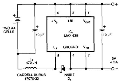
This Simple Hot-Lead Regulator Circuit Diagram derives 5 Vdc from 2-AA cells—even at their end-life voltages of 1.05 V, and is approximately 80% efficient, providing 5 V at 4 mA from 2.1 V at 11 mA. IC1 is manufactured by Maxim Integrated Products, Inc.


Hot-Lead Regulator Circuit Diagram

Simple

Here continue read..

Tuesday, December 24, 2013

High Voltage Regulator Circuit Diagram

The High Voltage Regulator Circuit Diagram delivers 100-V at 100 mA and withstands shorts to ground. Even at 100 V output, the LT317A functions in the normal mode, maintaining 1.2 V between its output and adjustment pin. Under these conditions, the 30-V zener is off and Ql conducts. When an output short occurs, the zener conducts, forcing Q1`s base to 30 V. 

This causes Q1`s emitter to clamp 2 VnEs below Vz. well within the V.w VouT rating of the regulator. Under these conditions, Q1, a high-voltage device, sustains 90 V-VcE at whatever current the transformer specified saturates at 130 mA, while Q1 safely dissipates 12 W. If Q1 and the LT317 A are thermally coupled, the regulator will soon go into thermal shutdown and oscillation will commence. 

This action will continue, protecting the load and the regulator as long as the output remains shorted. The 500-pF capacitor and the 10 0/0.02 11F damper aid transient response and the diodes provide safe discharge paths for the capacitors. 

High Voltage Regulator Circuit Diagram

High Voltage Regulator Circuit Diagram


Here continue read..

Monday, December 23, 2013

Simple Hot Lead Regulator Circuit Diagram

This Simple Hot-Lead Regulator Circuit Diagram derives 5 Vdc from 2-AA cells—even at their end-life voltages of 1.05 V, and is approximately 80% efficient, providing 5 V at 4 mA from 2.1 V at 11 mA. IC1 is manufactured by Maxim Integrated Products, Inc.


Hot-Lead Regulator Circuit Diagram

Simple Hot-Lead Regulator Circuit Diagram

Here continue read..

Digital Fan Regulator

The circuit presented here can be used to control the speed of  fans using induction motor. The speed control is nonlinear, i.e. in steps. The current step number is displayed on a 7-segment display. Speed can be varied over a wide range because the circuit can alter the voltage applied to the fan motor from 130V to 230V RMS in a maximum of seven steps.  The triac used in the final stage is fired at different angles to get different voltage outputs by applying short-dura-tion current pulses at its gate. For this pur-pose a UJT relax-ation oscillator is used that outputs sawtooth waveform. This waveform is coupled to the gate of the triac through an optocoupler (MOC3011) that has a triac driver output stage.

Pedestal voltage control is used for varying the firing angle of the triac. The power supply for the relaxation oscillator is derived from the rectified mains via 10-kilo-ohm, 10W series dropping/limit-ing resistor R2.  The pedestal voltage is derived from the non-filtered DC through optocoupler 4N33. The conductivity of the Darlington pair transistors inside this optocoupler is varied for getting the pedestal voltage. For this, the positive sup-ply to the LED inside the optocoupler is connected via different values of resistors using a multiplexer (CD4051).

Digital Fan Regulator Circuit diagram:
Digital Fan Regulator Circuit Diagram

The value of resistance selected by the multiplexer depends upon the control in-put from BCD up-/down-counter CD4510 (IC5), which, in turn, controls forward bi-asing of the transistor inside optocoupler 4N33. The same BCD outputs from IC5 are also connected to the BCD-to-7-seg-ment decoder to display the step number on a 7-segment display.  NAND gates N3 and N4 are config-ured as an astable multivibrator to produce rectangular clock pulses for IC5, while NAND gates N1 and N2 generate the active-low count enable (CE) input using either of push-to-on switches S1 or S2 for count up or count down operation, respectively, of the BCD counter.

Optocoupler 4N33 electrically isolates the high-voltage section and the digital section and thus prevents the user from shock hazard when using switches S1 and S2. BCD-to-7-segment decoder CD4543 is used for driving both common-cathode and common-anode 7-segment displays. If phase input pin 6 is ‘high’ the decoder works as a common-anode decoder, and if phase input pin 6 is ‘low’ it acts as a common-cathode decoder.  Optocoupler 4N33 may still conduct slightly even when the display is zero, i.e. pin 13 (X0, at ground level) is switched  output pin 3. To avoid this problem, adjust preset VR1 as required using a plastic-handled screwdriver to get no output at zero reading in the display.

Source :  http://www.ecircuitslab.com/2011/10/digital-fan-regulator.html


Here continue read..