Friday, December 27, 2013

TDA2030A 35W Amplifier used in Home Theaters

TDA2030A is a well used class AB audio amplifier IC. This one is mostly used in nowadays home theater systems for it’s some good features,
  1. Small size IC(package PENTAWATT V, almost size of regular TO220)
  2. Maximum voltage range (upto 44Volts Vs MAx)
  3. Very low harmonic and cross-over distortion.
  4. Suited for more reliable applications without regulated supply
  5. Up to 35Watts RMS driver output
  6. Thermal shutdown protection
This IC require less external components too, making it easier for a beginner to make this on veroboard. The original circuit I got from it’s datasheet. A little modified circuit below,

TDA2030A Amplifier used in Home Theaters

This can be operated with single supply line, but that topology gives less output power, hence this bi-voltage topology is used everywhere. We need to provide +/- 12V to it. We can easily get +12V and -12V from a 12-0-12 CT step down transformer. And, as this IC doesn’t require regulated supply, we can feed voltage directly from rectifier with just a capacitor. Well, the IC costs around 25 rupees, and together with all other materials as PCB, other parts the cost of final board doesn’t exceed 70-75 rupees.
Here continue read..

Circuit Guards Amplifier Outputs Against Overvoltage

A universal requirement for automotive electronics is that any device with direct connections to the wiring harness must be able to withstand shorts to the battery voltage. Though brutal, this requirement is necessary for reliability and for safety. One example of the need for this protection is an audio amplifier that produces indicator noises in the automotive interior. Though operating from a voltage of 3.3 or 5V, which is lower than the battery voltage, the amplifier must be able to stand off the full battery voltage.
Circuit diagram :
amplifier outputs against overvoltage
Figure 1 : This output circuit provides continuose protection against overvoltge faults
You can also use a protection network appropriate for these amplifiers for other automotive circuits (Figure 1). A dual N-channel MOSFET disconnects the amplifier’s outputs from the wiring harness in response to a high-voltage condition on either output. The MOSFETs, Q1A and Q1B, are normally on; zener diode D4 and its bias components drive the MOSFETs’ gates to approximately 11V. Dual diode D3 provides a diode-OR connection to the dc voltage on each output, thereby producing a voltage that controls the output of shunt regulator IC2. The circuitry protects IC1, a 1.4W Class AB amplifier suitable for audible warnings and indications for the automotive electronics.
During normal operation, the amplifier outputs’ dc components are at one-half of the VCC supply—2.5V in this case, for which VCC is 5V. The 11V gate drive fully enhances the MOSFETs, and the shunt-regulator output is off because its feedback input, Pin 5, is below its internal 0.6V threshold. If either output exceeds 5V, current flows through D3 into the R5/R6 divider, pulling the feedback terminal above its threshold. The shunt-regulator output then pulls the MOSFET-gate voltage from 11V almost to ground, which blocks high voltage from the amplifier by turning off the MOSFETs. The MOSFETs easily withstand the continuous output voltage, and the circuit returns to normal operation when you remove the short. Because the circuit does not respond instantaneously, zener diodes D1 and D2 provide protection at the beginning of a fault condition.
Figure 2. Figure 2. In Figure 1, one of U1s two audio outputs (top trace) is protected when its external terminal accidentally contacts an 18V supply voltage (2nd trace).

The waveforms of Figure 2 represent an operating circuit. One of the amplifier’s outputs (Trace 1) is a 1-kHz sine wave biased at a dc voltage of 2.5V. Trace 2 is the signal on the wire harness. It also starts as a 1-kHz sine wave biased at a 2.5V-dc voltage, but, at 200 µsec, it shorts to an 18V supply. Trace 3 is the shunt regulator’s output, initially biased at 11V but pulled to ground in response to the overvoltage condition. Trace 4 is current in the wire harness. Initially a sine wave, this current drops to zero in response to the overvoltage condition.
The components in Figure 1 optimize this circuit for 5V operation. For other voltages, you can adjust the R5/R6 resistor values. The shunt regulator must be able to function in saturation and, therefore, requires a separate supply pin in addition to the shunt output pin. The circuit repeatedly withstands 28V shorts without damage.

Source :   http://www.ecircuitslab.com/2012/06/circuit-guards-amplifier-outputs.html
Here continue read..

10 Band Equalizer

The equalizer presented in this article is suitable for use with hi-fi installations, public-address systems. mixers and electronic musical instruments. The relay contacts at the inputs and outputs, in conjunction with S2, enable the desired channel to be selected. The input may be linked directly to the output, if wanted. The input impedance and amplification of the equalizer are set with S1 and S3. The audio frequency spectrum of 31 Hz to 16 kHz is divided into ten bands. Ten bands require ten filters, of which nine are passive and one active. The passive filters are identical in design and differ only in the value of the relevant inductors and capacitors. The requisite characteristics of the filters are achieved by series and parallel networks.

The filter for the lowest frequency band is an active one to avoid a very large value of inductance. It is based in a traditional manner on op amp A1. The inductors used in the passive filters are readily available small chokes. The filter based on L1 and L2 operates at about the lowest frequency (62 Hz) that can be achieved with standard, passive components. The Q(uality) factor of the filters can, in principle, be raised slightly by increasing the value of R19 and R23, as well as that of P1–P10, but that would be at the expense of the noise level of op amp IC1. With component values as specified, the control range is about ±11 dB, which in most case will be fine. A much larger range is not attainable without major redesign.

10-Band Equalizer Circuit diagram:


The input level can be adjusted with P1, which may be necessary for adjusting the balance between the channels or when a loudness control is used in the output amplifiers. Several types of op amp can be used:in the prototype, IC1 is an LT1007, and IC2, an OP275. Other suitable types for IC1 are OP27 or NE5534; and for IC2, AD712, LM833 and NE5532. If an NE5534 is used for IC1, C2 is needed; in all other cases, not. The circuit needs to be powered by a regulated, symmetrical 15 V supply. It draws a current of not more than about 10mA.
Source : http://www.ecircuitslab.com/2011/05/10-band-equalizer.html
Here continue read..

Battery powered Headphone Amplifier

Low distortion Class-B circuitry 6V Battery Supply

Some lovers of High Fidelity headphone listening prefer the use of battery powered headphone amplifiers, not only for portable units but also for home "table" applications. This design is intended to fulfil their needs and its topology is derived from the Portable Headphone Amplifier featuring an NPN/PNP compound pair emitter follower output stage. An improved output driving capability is gained by making this a push-pull Class-B arrangement. Output power can reach 100mW RMS into a 16 Ohm load at 6V supply with low standing and mean current consumption, allowing long battery duration. The single voltage gain stage allows the easy implementation of a shunt-feedback circuitry giving excellent frequency stability.

Battery-powered Headphone Amplifier Circuit diagram

Notes:
  • For a Stereo version of this circuit, all parts must be doubled except P1, SW1, J2 and B1.
  • Before setting quiescent current rotate the volume control P1 to the minimum, Trimmer R6 to maximum resistance and Trimmer R3 to about the middle of its travel.
  • Connect a suitable headphone set or, better, a 33 Ohm 1/2W resistor to the amplifier output.
  • Switch on the supply and measure the battery voltage with a Multimeter set to about 10Vdc fsd.
  • Connect the Multimeter across the positive end of C4 and the negative ground.
  • Rotate R3 in order to read on the Multimeter display exactly half of the battery voltage previously measured.
  • Switch off the supply, disconnect the Multimeter and reconnect it, set to measure about 10mA fsd, in series to the positive supply of the amplifier.
  • Switch on the supply and rotate R6 slowly until a reading of about 3mA is displayed.
  • Check again the voltage at the positive end of C4 and readjust R3 if necessary.
  • Wait about 15 minutes, watch if the current is varying and readjust if necessary.
  • Those lucky enough to reach an oscilloscope and a 1KHz sine wave generator, can drive the amplifier to the maximum output power and adjust R3 in order to obtain a symmetrical clipping of the sine wave displayed.
Technical data:
Output power (1KHz sinewave):
    16 Ohm: 100mW RMS
    32 Ohm: 60mW RMS
    64 Ohm: 35mW RMS
    100 Ohm: 22.5mW RMS
    300 Ohm: 8.5mW RMS
Sensitivity:
    160mV input for 1V RMS output into 32 Ohm load (31mW)
    200mV input for 1.27V RMS output into 32 Ohm load (50mW)
Frequency response @ 1V RMS:
    flat from 45Hz to 20KHz, -1dB @ 35Hz, -2dB @ 24Hz
Total harmonic distortion into 16 Ohm load @ 1KHz:
    1V RMS (62mW) 0.015% 1.27V RMS (onset of clipping, 100mW) 0.04%
Total harmonic distortion into 16 Ohm load @ 10KHz:
    1V RMS (62mW) 0.05% 1.27V RMS (onset of clipping, 100mW) 0.1%
Unconditionally stable on capacitive loads
Source :  http://www.ecircuitslab.com/2012/04/battery-powered-headphone-amplifier.html
Here continue read..

Modular Phono Preamplifier

High Quality Moving Magnet Pick-up module, Two-stage Series/Shunt feedback RIAA equalization
Any electronics amateur still in possess of a collection of vinyl recordings and aiming at a high quality reproduction should build this preamp and add it to the Modular Preamplifier chain. This circuit features a very high input overload capability, very low distortion and accurate reproduction of the RIAA equalization curve, thanks to a two-stage op-amp circuitry in which the RIAA equalization network was split in two halves: an input stage (IC1A) wired in a series feedback configuration, implementing the bass-boost part of the RIAA equalization curve and a second stage, implementing the treble-cut part of the curve by means of a second op-amp (IC2A) wired in the shunt feedback configuration.

This module comprises also an independent dual rail power supply identical to that described in the Modular Preamplifier Control Center. As with the other modules of this series, each electronic board can be fitted into a standard enclosure: Hammond extruded aluminum cases are well suited to host the boards of this preamp. In particular, the cases sized 16 x 10.3 x 5.3 cm or 22 x 10.3 x 5.3 cm have a very good look when stacked. See below an example of the possible arrangement of the rear panel of this module.

Modular Phono Preamplifier Circuit diagram:
Modular Phono Preamplifier Circuit Diagram

Parts:
R1_____________270R 1/4W Resistor
R2_____________100K 1/4W Resistor
R3_____________2K2 1/4W Resistor
R4_____________39K 1/4W Resistor
R5_____________3K9 1/4W Resistor
R6_____________390K 1/4W Resistor
R7_____________33K 1/4W Resistor
R8_____________75K 1/4W Resistor (or two 150K resistors wired in parallel)
R9_____________560R 1/4W Resistor
C1_____________220pF 63V Polystyrene or Ceramic Capacitor
C2_____________1µF 63V Polyester Capacitor
C3_____________47µF 25V Electrolytic Capacitor
C4_____________10nF 63V Polyester Capacitor 5% tolerance or better
C5_____________1nF 63V Polyester Capacitor 5% tolerance or better
C6,C9__________100nF 63V Polyester Capacitors
C7,C10_________22µF 25V Electrolytic Capacitors
C8,C11_________2200µF 25V Electrolytic Capacitors
IC1____________LM833 or NE5532 Low noise Dual Op-amp
IC2____________TL072 Dual BIFET Op-Amp
IC3____________78L15 15V 100mA Positive Regulator IC
IC4____________79L15 15V 100mA Negative Regulator IC
D1,D2_________1N4002 200V 1A Diodes
J1,J2__________RCA audio input sockets
J3_____________Mini DC Power Socket

Notes:
  • The circuit diagram shows the Left channel only and the power supply
  • Some parts are in common to both channels and must not be doubled. These parts are: IC3, IC4, C6, C7, C8, C9, C10, C11, D1, D2 and J3.
  • IC1 and IC2 are dual Op-Amps, therefore the second half of these devices will be used for the Right channel
  • This module requires an external 15 - 18V ac (50mA minimum) Power Supply Adaptor.
Technical data:
Sensitivity @ 1KHz: 4.3mV RMS input for 200mV RMS output
Max. input voltage @ 100Hz: 53mV RMS
Max. input voltage @ 1KHz: 212mV RMS
Max. input voltage @ 10KHz: 477mV RMS
Frequency response @ 200mV RMS output: flat from 30Hz to 23KHz; -0.5dB @ 20Hz
Total harmonic distortion @ 1KHz and up to 8.8V RMS output: 0.0028%
Total harmonic distortion @10KHz and up to 4.4V RMS output: 0.008%

Source :  http://www.ecircuitslab.com/2011/06/modular-phono-preamplifier.html
Here continue read..

Thursday, December 26, 2013

Battery Discharger

The battery discharger published in this website may be improved by adding a Schottky diode (D3). This ensures that a NiCd cell is discharged not to 0.6–0.7 V, but to just under 1 V as recommended by the manufacturers. An additional effect is then that light-emitting diode D2 flashes when the battery connected to the terminals is flat. The circuit in the diagram is based on an astable multivibrator operating at a frequency of about 25 kHz.

When transistor T2 conducts, a current flows through inductor L1, whereupon energy is stored in the resulting electromagnetic field. When T2 is cut off, the field collapses, whereupon a counter-emf is produced at a level that exceeds the forward voltage (about 1.6 V) of D2. A current then flows through the diode so that this lights. Diode D1 prevents the current flowing through R4 and C2. This process is halted only when the battery voltage no longer provides a sufficient base potential for the transistors.

Battery Discharger Circuit Diagram

In the original circuit, this happened at about 0.65 V. The addition of the forward bias of D3 (about 0.3 V), the final discharge voltage of the battery is raised to 0.9–1.0 V. Additional resistors R5 and R6 ensure that sufficient current flows through D3. When the battery is discharged to the recommended level, it must be removed from the discharger since, in contrast to the original circuit, a small current continues to flow through D3, R2-R3, and R5-R6 until the battery is totally discharged.

The flashing of D2 when the battery is nearing recommended discharge is caused by the increasing internal resistance of the battery lowering the terminal voltage to below the threshold level. If no current flows, the internal resistance is of no consequence since the terminal voltage rises to the threshold voltage by taking some energy from the battery. When the discharge is complete to the recommended level, the LED goes out. It should therefore be noted that the battery is discharged sufficiently when the LED begins to flash.

Here continue read..

Build a Switch Mode Power Supply

The SMPS described here is suit-able for high-wattage stereos and other similar equipment. The circuit employs two high-voltage power transistors (BU208D) which have built-in re-verse-connected di-odes across their collectors and emitters. It can supply about 250-watt out-put. The circuit uses a ferrite core transformer of 14mm width, 20mm height, and 42mm length of E-E cores. An air gap of 0.5 mm is required between E-E junction. Good insulation using plastic-insulating sheets (Mylar) is to be maintained between each layer of winding.

 Switch Mode Power Supply Circuit Diagram
 
 Switch Mode Power Supply Circuit Diagram

The number of primary turns required is 90 with 26 SWG wire. The secondary winding employs 17 SWG wire (for 4A load current). Each turn of the secondary develops approximately 2 volts. The reader can decide about the output volt-age and the corresponding secondary turns, which would work out to be half the desired secondary voltage. The volt-age rating of capacitors C7 and C8 should be at least twice the secondary output of each secondary section. BY396 rectifier diodes shown on the secondary side can be used for a maximum load current of 3 amperes.

Two feedback windings (L1 and L2) using two turns each of 19 SWG wire are wound on the same core. These windings are connected to transistors T1 and T2 with a phase difference of 180o,  as shown by the polarity dots in the figure. First wind the primary winding (90 turns using 26 SWG wire) on the former. Then wind the two feedback windings over the secondary (output). Ensure that each winding is separated by an insulation layer.  Two separate heat sinks are to be pro-vided for the two transistors (BU208D).

The filter capacitor for mains should be of at least 47µF, 350V rating. It is better to use a 100µF, 350V capacitor. If the output is short-circuited by less than 8-ohm load, the SMPS would automatically turn off because of the absence of base current.  The hfe min (current amplification factor) of BU208D is 2.5. Thus, sufficien base current is required for fully satu rated operation, otherwise the transistors get over-heated. At times, due to use of very high value of capacitors C7 and C8 (say 2200mF or so) on the secondary side or due to low load, the oscillations may cease on the primary side. This can be rectified by increasing the value of capacitor C6 to 0.01mF.

Author :  Deepu P.A
Here continue read..

ELECTRONIC STOP WATCH

     Here is a simple circuit which can be used as an accurate stop-watch to count up to 100 seconds with a resolution of 0.01 second or up to 1000 seconds with a resolution of 0.1 second. This stop-watch can be used for sports and similar other activities.

     A 1MHz crystal generates stable frequency which is divided by two stages of 74390 ICs (dual decade counter) and another stage employing 7490 (decade counter) IC to obtain a final frequency of 100 Hz or 10 Hz. Due to the use of crystal, the final frequency is very accurate.

     The output of IC4 (7490) is counted and displayed using IC5 74C926 (4-digit counter with multiplexed 7-segment LED driver). Due to multiplexed display the power consumption is very low. Switch S2 (2-pole, 2-way) is used to select appropriate input frequency and corresponding decimal point position to display up to either 99.99 seconds or 999.9 seconds maximum count.

     For proper operation, first press switch S3 (reset) and then operate switch S2, according to the resolution/range desired (0.1 sec. or 0.01 sec.)/(100 seconds or 1000 seconds). Now to start counting, press switch S1. To stop counting, press switch S1 again. The counting will stop and display will show the correct time elapsed since the start of counting.


Here continue read..

Power Buzzer

How often on average do you have to call members of your family each day to tell them that dinner is ready, it’s time to leave, and the like? The person you want is usually in a different room, such as the hobby room or bedroom. A powerful buzzer in the room, combined with a pushbutton at the bottom of the stairs or in the kitchen, could be very handy in such situations. The heart of this circuit is formed by IC1, a TDA2030. This IC has built-in thermal protection, so it’s not likely to quickly give up the ghost. R1 and R2 apply a voltage equal to half the supply voltage to the plus input of the opamp. R3 provides positive feedback. Finally, the combination of C2, R4 and trimmer P12 determines the oscillation frequency of the circuit.

Power Buzzer Circuit diagram:

Power_Buzzer_Circuit_Diagram
Power Buzzer Circuit Diagram

The frequency of the tone can also be adjusted using P1. There is no volume control, since you always want to get attention when you press pushbutton S1. Fit the entire circuit where you want to have the pushbutton. The loudspeaker can then be placed in a strategic location, such as in the bedroom or wherever is appropriate. Use speaker cable to connect the loudspeaker. Normal bell wire can cause a significant power loss if the loudspeaker is relatively far away. The loudspeaker must be able to handle a continuous power of at least 6 W (with a 20-V supply voltage).

The power quickly drops as the supply voltage decreases (P = Urms 2 / RL). The power supply for this circuit is not particularly critical. However, it must be able to provide sufficient current. A good nominal value is around 400 mA at 20 V. At 4 V, it will be approximately 25 mA. Most likely, you can find a suitable power supply somewhere in your hobby room. Otherwise, you can certainly find a low-cost power supply design in our circuits archive that will fill the bill!

Source: http://www.ecircuitslab.com/2011/05/power-buzzer-circuit.html
Here continue read..

Pc Temperature Alarm

If your PC overheats, it could damage its expensive components. Here’s a circuit that warns you of your PC getting heated. Today’s computers contain most of the circuitry on just a few chips and reduced power consumption is a byproduct of this LSI and VSLI approach. Some PCs still have power supplies that are capable of supplying around 200W, but few PCs actually consume power to this extent.

On the other hand, apart from some portable and small desktop computers that use the latest micro-power components, most PCs still consume significant amount of power and generate certain amount of heat.  The temperature inside the aver-age PC starts to rise well above the ambient temperature soon after it is switched on. Some of the larger integrated circuits become quite hot and if the temperature inside the PC rises too high, these devices may not be able to dissipate heat fast enough. This, in turn, could lead to failure of devices and eventually of the PC.  Various means to combat overheating are available, ranging from simple temperature alarms to devices like temperature-activated fans to keep the microprocessor cool.

Here is a temperature alarm that activates an audio ‘beeper’ if the temperature inside the PC exceeds a preset threshold. This temperature is user-adjustable and can be anywhere between 0°C and 100°C.  The unit is in the form of a small PC expansion card, which you simply need to plug into any avail-able slot of the host PC. It is powered from the PC and consumes only about 12 mA.  The sensor (LM35) used here pro-vides a substantial amount of on-chip signal conditioning, including amplification, level shifting and phase in-version. As a result, it provides an out-put of 10 mV per degree centigrade rise in temperature. It caters to a temperature measurement range of 0°C to 100°C, which corresponds to 0V to 1V of voltage.

Pc Temperature Alarm Circuit Diagram

Pc Temperature Alarm-Circuit Diagram

The voltage-detector stage com-pares the output voltage of the temperature sensor with the preset reference voltage. The output of the comparator goes high if the output potential from the sensor exceeds the reference voltage. When this happens, the voltage comparator enables a low-frequency oscillator, which, in turn, activates the audio oscillator. The out-put of the audio oscillator is connected to a loudspeaker (LS1), which sounds a simple ‘beep-beep’ alarm. The reference voltage determines the temperature at which the alarm is activated.

Fig. 1 shows the circuit of the PC temperature alarm and Fig. 2 shows the pin configuration of sensor LM35. IC LM35 (IC1) is an easy-to-use temperature sensor. It is basically a three-terminal device (two supply leads plus the output) that operates over a wide supply range of 4 to 20V. It consumes only 56 µA at 5V and generates insignificant heat.

IC2 is an operational amplifier used here as a voltage comparator. VR1 pro- vides a reference voltage that can be set anywhere from 0V to approximately 1V, which matches the output voltage range of IC1. This reference voltage is applied to the inverting in- put of IC2 and the output of IC1 is coupled to the non-inverting input. Consequently, the output of IC2 is low if the output of IC1 is below the reference voltage, or high if the output of IC1 exceeds the reference voltage.

Pin details of LM35

Pin

The low-frequency oscillator IC3 is a standard 555 astable multivibrator circuit. It is gated via the reset input at pin 4, which holds output pin 3 low when IC3 is gated ‘off’ (when the out-put of IC2 is low). This prevents IC4 from oscillating. IC4 is another 555 astable multivibrator circuit, gated via its reset input. It has an operating frequency of approximately 2.5 kHz.  When IC3 is activated, its output pro-vides a square wave of 1 Hz. This is used to trigger IC4, which gives an audio output of 2.5 kHz in bursts. It is connected to loudspeaker LS1 to generate alarm.

The alarm circuit can be fitted into any spare expansion slot of the PC, but be careful to fit it the right way round. Before setting VR1 to a suitable thresh-old temperature, decide what that temperature should be. The technical specification in your computer’s manual might be of help here.  If we assume that the room temperature will not normally exceed 25oC, the temperature of the interior of the computer would be up to 35oC. Unless you have good reason to use a different threshold temperature, VR1 should be set for a wiper potential of 350 mV.

Trial-and-error method can be used in the absence of test equipment to enable VR1, but it would be a bit time-consuming. There is a slight complication in that the computer’s outer casing must be at least partially removed to provide access to VR1. Once VR1 has been adjusted, the outer casing must be put back into place so that the interior of the computer can warm up in the normal way. You must therefore al-low time for the temperature inside the computer to rise back to its nor-mal operating level each time VR1 is readjusted.

Source:  http://www.ecircuitslab.com/2012/05/pc-temperature-alarm.html
Here continue read..

Wednesday, December 25, 2013

Automobile White LED Light

Without any dedicated buck converter/white LED driver IC, you can safely drive many standard Hi-efficient white LED modules using the battery power available in automobiles. Here is a safe and simple white LED driver designed for 12V automobiles.

Auto White LED Circuit Schematic
Circuit Project: Automobile White LED Light


In the Automobile White LED Light circuit, fixed voltage regulator IC1 (7805) provides a steady voltage of 5V across C2. Resistors R1 limits the current flow through the white LED D1 (3v6/350mA) with the help of transistor T1 (and T2), ie components R1, T1 (and T2) provide a constant current to D1. Use a good heat sink for T1. This LED unit gives a constant light output for input voltages ranging from 8 to 18 volts!

Circuit Source: DIY Electronics Projects
Here continue read..

The component of mobile phone jammer is separate

The component of mobile phone jammer is separate.
In Nokias share of nearly 40% behind, hidden in its mobile phone sales channels infighting. Of the Nokia mobile phone sales channels, the channel model of the mobile phone industry is broadly divided into the national agency system, the provincial agency, the manufacturers supply model, first proposed by Nokia provincial direct control of distribution of Nokia mobile phone sales channels mode. Nokia mobile agents Postel and Telling, and last year the introduction of Synnex Technology International. We can find, continuously reported in the first half of this year, Nokia channels to dissatisfaction with the low gross margin and resentment.
The omnidirectional antenna of mobile phone jammer can be provided at different price.
Nanjing Panda Mobile Communications Equipment Co., Ltd. (abbreviation PMC). This is a mobile phone sales, R & D, production, sales and technical service in one enterprise. The company has set up 20 branches in Jiangsu, Sichuan, northeast, Guangdong, Shanghai, Beijing, formed based in Jiangsu, echoing the north and south, radiation thing, the market, sales, business-linked target sales network to expand its market share and actively to expand overseas. According to the Nanjing Panda 2003, its total mobile phone sales in the first half of 2003 of 1.306 billion yuan, ranked fifth in the domestic mobile phone. However, according to latest data released in early April 2004. This mobile phone jammer system has the anti-damage protection function.
Chinese mobile phone an annual capacity of 2004 exceeded 170 million mark, while the total market capacity is only 69 million units, the middle will have to deduction of no small proportion of the mobile phone market (in Guangzhou and other places, and second, the proportion of a conservative estimate more than 20%). According to the view of modern marketing, product characteristics is a key factor in the impact of marketing decisions. So a study of the mobile marketing channel to start from the phones features and marketing features. Phone as a convenient communication tool, has its own characteristics. First of all, the phones main function is the most basic function of communication. With the development of society, an increasingly wide range of peoples activities, the concept of global village has long been popular. It can prevent the intentional and unintentional damage to mobile phone jammer .
Here continue read..

Solar Powered SLA Battery Maintenance

This circuit was designed to ‘baby-sit’ SLA (sealed lead-acid or ‘gel’) batteries using freely available solar power. SLA batteries suffer from relatively high internal energy loss which is not normally a problem until you go on holidays and disconnect them from their trickle current charger. In some cases, the absence of trickle charging current may cause SLA batteries to go completely flat within a few weeks. The circuit shown here is intended to prevent this from happening. Two 3-volt solar panels, each shunted by a diode to bypass them when no electricity is generated, power a MAX762 step-up voltage converter IC.

Solar Powered SLA Battery Maintenance Circuit Diagram
Solar Powered SLA Battery-Maintenance-Circuit-Diagram

The ‘762 is the 15-volt-out version of the perhaps more familiar MAX761 (12 V out) and is used here to boost 6 V to 15 V.C1 and C2 are decoupling capacitors that suppress high and low frequency spurious components produced by the switch-mode regulator IC. Using Schottky diode D3, energy is stored in inductor L1 in the form of a magnetic field. When pin 7 of IC1 is open-circuited by the internal switching signal, the stored energy is diverted to the 15-volt output of the circuit. The V+ (sense) input of the MAX762, pin 8, is used to maintain the output voltage at 15 V. C4 and C5 serve to keep the ripple on the output voltage as small as possible. R1, LED D4 and pushbutton S1 allow you to check the presence of the 15-V output voltage.

D5 and D6 reduce the 15-volts to about 13.6 V which is a frequently quoted nominal standby trickle charging voltage for SLA batteries. This corresponds well with the IC’s maximum, internally limited, output current of about 120 mA. The value of inductor L1 is not critical — 22 µH or 47 µH will also work fine. The coil has to be rated at 1 A though in view of the peak current through it. The switching frequency is about 300 kHz. A suggestion for a practical coil is type M from the WEPD series supplied by Würth (www.we-online.com). Remarkably, Würth supply one-off inductors to individual customers. At the time of writing, it was possible, under certain conditions, to obtain samples, or order small quantities, of the MAX762 IC through the Maxim website at www.maxim-ic.com.

Source: http://www.ecircuitslab.com/2011/12/solar-powered-sla-battery-maintenance.html 
Here continue read..

3 3V And 5V Outputs Dc Dc Converter Circuit Diagram
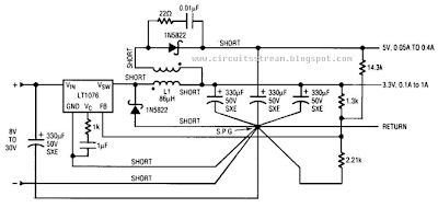
This is the 3.3V And 5V Outputs - Dc-Dc Converter Circuit Diagram. This Input, voltages can range from 8 V to 30 V. The load range on the 5 V is 0,05 A to 5 A while the 3.3-V load range is 0.1 A to 1 A. The circuit is self-protected under no-load conditions. Over all load and line conditions, .including cross regulation, the 3.3-V output varies from 3.25 V to 3.27 V. The 5-V output varies from 4.81 V to 5.19 V under the same conditions. 

In a typical application to 0.5 A on the 3.3 V and 0.25 A on the 5 V, efficiency is typically 76%, With an input voltage of 30 V and a full-load condition, the efficiency drops to 66%. In normal operating regions, efficiency is always better than 70%.The 5-V ripple is less than 75 mV and the 3.3-V ripple less than 50 mV over all line and load conditions.

3.3V And 5V Outputs - Dc-Dc Converter Circuit Diagram

3.3V And 5V Outputs - Dc-Dc Converter Circuit Diagram

Here continue read..

Tuesday, December 24, 2013

High Voltage Regulator Circuit Diagram

The High Voltage Regulator Circuit Diagram delivers 100-V at 100 mA and withstands shorts to ground. Even at 100 V output, the LT317A functions in the normal mode, maintaining 1.2 V between its output and adjustment pin. Under these conditions, the 30-V zener is off and Ql conducts. When an output short occurs, the zener conducts, forcing Q1`s base to 30 V. 

This causes Q1`s emitter to clamp 2 VnEs below Vz. well within the V.w VouT rating of the regulator. Under these conditions, Q1, a high-voltage device, sustains 90 V-VcE at whatever current the transformer specified saturates at 130 mA, while Q1 safely dissipates 12 W. If Q1 and the LT317 A are thermally coupled, the regulator will soon go into thermal shutdown and oscillation will commence. 

This action will continue, protecting the load and the regulator as long as the output remains shorted. The 500-pF capacitor and the 10 0/0.02 11F damper aid transient response and the diodes provide safe discharge paths for the capacitors. 

High Voltage Regulator Circuit Diagram

High Voltage Regulator Circuit Diagram


Here continue read..

Security System Switcher

An audio signal can be used as a form of input to control any security system. For example, an automatic security camera can be configured to respond to a knock on the door. The circuit described here allows the security system to automatic in on state. It uses a transducer to detect intruders and a 5V regulated DC power supply provides power to the circuit.

As shown in Fig. 1, a condenser microphone is connected to the input of small signal Pre- amplifier built around transistor T1. Biasing resistor R1 determines to a large extent the microphone sensitivity. A microphone usually has an internal FET which requires a bias voltage to operate. The sound picked up by the microphone is amplified and fed to input pin 2 of IC1 (LMC555) wired in monostable configuration.

Fig. 1: Schematic Security system switcher Circuit diagram :

Schematic Security system switcher-Circuit Diagram


IC2 (CD4538B) is a dual, precision monostable multivibrator with independent trigger and reset controls. The output of IC1 is connected to the first trigger input pin 4 of IC2(A) through switch S1. If an intruder opens or breaks the door, IC1 is triggered by sound signals; the timer output pin 3 of IC1 goes high and enables first monostable multivibrator IC2(A). IC2(A) provides a time period of around 5 to 125 seconds, which is adjusted with preset VR1.

Another monostable multivibrator IC2(B) also provides a time period of around 25 to 600 seconds, which is adjusted with preset VR2. The output of IC2(B) is used to energise relay RL1. Indicator LED1 is provided to display the relay activity. Any AC/DC operated security gadget is activated or deactivated through a security switch. Thus, the security switch of the gadget is connected in the n/o contacts of the relay.You can also operate high power beacons, sirens or hooters in place of the security switch for any AC/DC operated security gadget.

Fig. 2: Proposed cabinet :
Proposed cabinet


Assemble the circuit on a general-purpose PCB and enclose it in a cabinet as shown in Fig. 2 along with 5V adaptor for powering the circuit. Connect the security switch according to the circuit diagram and use appropriate AC/DC power supply required to operate the security gadget.

Warning! All relevant electrical safety precautions should be taken when connecting mains power supply to the relay contacts. With the help of single pole double throw (SPDT) switch S1, internal or external trigger input (active high signal) can be selected.


Here continue read..

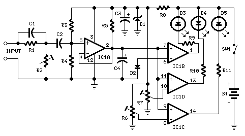
25W Three Level Audio Power Indicator

This circuit is intended to indicate the power output level of any audio amplifier. It is simple, portable, and displays three power levels that can be set to any desired value. For a standard Hi-Fi stereo power amplifier like the 25W one described in these pages, the power output values suggested are as followings:
  • D5 illuminates at 2W
  • D4 illuminates at 12.5W
  • D3 illuminates at 24.5W
The above values were chosen for easy setup, but other settings are possible. IC1A is the input buffer, feeding 3 voltage comparators and LEDs drivers by means of a variable dc voltage obtained by R5 and C4 smoothing action. In order to achieve setting stability, the supply of IC1 and trimmers R6 & R7 is reduced and clamped to 5.1V by Zener diode D1.

25W - Three Level Audio Power Indicator
2W, 12.5W, 24.5W - Three Level Audio Power Indicator Circuit Diagram

Parts:


  • R1 100K 1/4W Resistor
  • R2 50K 1/2W Trimmer Cermet
  • R3 330K 1/4W Resistor
  • R4 1M2 1/4W Resistor
  • R5 470K 1/4W Resistor
  • R6,R7 500K 1/2W Trimmers Cermet
  • R8 1K5 1/4W Resistor
  • R9-R11 470R 1/4W Resistors
  • C1 47pF 63V Ceramic Capacitor
  • C2 100nF 63V Polyester Capacitor
  • C3 47µF 25V Electrolytic Capacitor
  • C4 1µF 25V Electrolytic Capacitor
  • D1 BZX79C5V1 5.1V 500mW Zener Diode
  • D2 1N4148 75V 150mA Diode
  • D3-D5 3mm. Yellow LEDs
  • IC1 LM339 Quad Voltage Comparator IC
  • SW1 SPST Slider Switch
  • B1 9V PP3
  • Clip for 9V PP3 Battery

Notes:


  1. The simplest way to connect this circuit to the amplifier output is to use a twisted pair cable terminated with two insulated crocodile clips.
  2. Setup is best accomplished with an oscilloscope or an audio millivoltmeter like the one described in these pages.
  3. A 1KHz sine wave generator with variable output is also required (see a suitable circuit in this website also).
  4. Connect the generator to the amplifier input and the Audio Power Indicator to the output of the amplifier, in parallel with the oscilloscope probe or the audio millivoltmeter input.
  5. When using high power outputs disconnect the loudspeakers to avoid Tweeters damage and connect in their place an 8 Ohm 20-30 Watt wirewound resistor.
  6. Remember that VRMS output is equal to output Peak-to-Peak Voltage divided by 2.828.
  7. RMS power output in Watts is equal to VRMS2 divided by speaker impedance (usually 8 or 4 Ohms).
  8. Example: set the output of the 1KHz sinewave generator to read 14V on the audio millivoltmeter (24.5W 8 Ohms). Set R2 until D3 illuminates, and be sure that D3 turns-off when diminishing a little the generators output.
  9. Do the same with R7 for D4 and R6 for D5. The readings of the audio millivoltmeter must be 10V (12.5W 8 Ohms) and 4V (2W 8 Ohms) respectively.
Here continue read..

Automotive Speed Indicator

The speed of an automobile can be indicated by detecting the pulses generated by the ignition system and causing an LED to light. The circuit utilizes a quad NOR gate IC chip. Two of the gates are configured as a one shot multivibrator which produces a fixed duration pulse each time the primary circuit of the automobile ignition system opens the circuit to the ignition coil. The other 2 gates are used as buffers which provide an accurate rectangle pulse.

As the number of pulses per second increases, the voltage fed to the base of of the NPN transistor becomes high enough to cause it to conduct and turn on the LED. The speed at which the LED lights is set by R4. The input of the circuit is connected to the distributor side of the ignition coil or to the tachometer connection on those cars that are equipped with electronic ignition.
Here continue read..

12Volt to 9Volt DC Converter

To get a more precise output voltage, replace zener diode Z1 with 10V and R1 with a 1Kilo ohm potentiometer. A Coolrib for Q1 is optional but highly recommended. You can replace Q1 for a more robust type to get more output amps depending on your requirements. Simple circuit to power your 9 volt cassette recorder and other stuff.


Parts List:
R1 = 560 ohm
C1 = 1000uF/40V, Electrolytic
C2 = 10uF/25V, Electrolytic
C3 = 330nF, Ceramic
Z1 = 9.1V, 1watt zener
Q1 = ECG184, NTE184
Here continue read..

Build A Homemade Fence Charger Energizer Circuit Explained

The electric fence charger circuit presented here is basically a high voltage pulse generator. The super high voltage is derived from a commonly used automobile ignition coil. An a stable multivibrator is used to generate the required frequency to drive the ignition coil. Another a stable is used to control the pulses supplied to the fence.

 If you have large agricultural fields and desperately need to protect the crops from uninvited guests like animals and possibly humans, then this electric fence charger device is just what you are looking for. Build and install it yourself. An electric fence is an electrified high voltage barrier which produces painful shocks if physically touched or manipulated. Thus such fencing basically function as deterrents for animals as well as human intruders and stop them from crossing the restricted boundary.

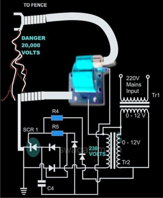
Build  A Homemade Fence Charger Energizer Circuit Explained

Build  A Homemade Fence Charger Energizer Circuit Explained


The present circuit of an electric fence charger is designed and tested by me and has proved sufficiently powerful for the application. The circuit is able to produce voltage pulses up to 20,000 volts, needless to say about the fatality rate involved with it. However the pulses being intermittent, provides the subject with enough time to realize, recover and eject.

The generated pulse is so powerful that it can easily arc and fly-off between short distances of around a cm. so the fencing conductor needs to be separated adequately to avoid leakages through arcing and sparking. If not tackled, may drastically reduce the effectiveness of the unit.

Here the generation of high voltage is primarily carried out by an automobile ignition coil.

The winding ratios of an ignition coil are specifically designed and intended for creating high voltage arc between a two closely spaced conductors inside the ignition chamber to initiate the ignition process in vehicles.

Basically it’s just a step-up transformer, which is able to step-up an input applied voltage at its primary winding to monstrous levels at its output or the secondary winding.

SOME POINTS OF THE CIRCUIT AND THE IGNITION COIL IS VERY DANGEROUS TO TOUCH WHEN POWERED. ESPECIALLY THE IGNITION COIL OUTPUT IS TOO LETHAL AND MAY EVEN CAUSE PARALYSIS.

Let’s diagnose the whole thing more deeply.

Circuit Description


In the CIRCUIT DIAGRAMwe see that the entire circuit is basically comprised of four stages.

A DC oscillator stage, An intermediate 12 to 230 volts step-up stage, The voltage collector and firing stage and The super high voltage-booster stage.

 TR1 and TR2 are two normal step-down transformers whose secondary windings are connected through SCR2. TR2’s input primary winding may be selected as per the country specification.

However, TR1’s primary should be rated at 230 volts.

IC1 along with the associated components forms a normal astable multivibrator stage. The supply voltage to the circuit is derived from the secondary of TR2 itself.

The output from the astable is used to trigger SCR2 and the whole system, at a particular fixed intermittent rate as per the settings of P1.

During the ON periods, SCR2 connects the 12 volt AC from TR2 to the secondary of TR1 so that a 230 volt potential instantly becomes available at the other end of TR1.

 This voltage is fed to the voltage-firing stage consisting of the SCR1 as the main active component along with a few diodes, resistor and the capacitor C4.

The fired voltage from SCR1 is dumped into the primary winding of the ignition coil, where it is instantly pulled to a massive 20,000 volts at its secondary winding. This voltage may be suitably terminated into the fencing.

The high voltage generated by this electric fence charger will need to be carefully applied across the whole length of the fence.

The two poles from the ignition coil connected to the fence wiring should be kept at least 2 inches apart.

 The pillars of the fence should be ideally made of plastic or similar non conducting material, never use metal and not even wood (wood tend to absorb moisture and may give path to leakages).

 Parts List

R4 = 1K, 1WATT,
R5 = 100 OHMS, 1WATT,
P1 = 27K PRESET
C4 = 105/400V PPC,
ALL DIODES ARE 1N4007,
IC = 555
TR1 = 0-12V/3Amp (120 or 230V)
TR2 = 0-12V/1Amp (120 or 230V)
BOTH THE SCRs ARE C106 OR PREFERABLY BT151,

TWO WHEELER IGNITION COIL IS SHOWN IN FLUORESCENT BLUE COLOR

Here continue read..

Monday, December 23, 2013

Multi Color LED

How many different conditions do you reckon may be signalled with just one LED? Two, maybe three? Using this simple circuit, a lot more! Admittedly, a two-colour LED is used here. Such a device consists of two light-emitting chips, usually red and green, encapsulated in the same case. It has three pins: two for the anodes, and one for the common cathode. In this way, each diode can be activated separately. Various mixed colours may be obtained by varying the current through the two diodes. At least four discrete colours are then easily perceived: pure red, pure green, orange (I R ≈ 2 I G ) and yellow (I G ≈ 2I R ).

In the present circuit, the LED elements are driven by CMOS three-state buffers type 4503, which, unlike most CMOS ICs from the 4000 series, are capable of supplying up to 10 mA of output current. The LED cur-rents are limited by resistors R1 through R6, whose values invite experiments with brightness and colours according to your own taste.

Circuit diagram :

Multi-Color LED-Circuit Diagram

Multi-Color LED Circuit Diagram

The circuit was originally developed to indicate the state of three inputs, a, b, and c (non-binary, i. e., only one of these is at 1 at any time), with the coniguration (a=b=c=0) representing the fourth state. The latter is decoded by NAND gate IC1. An additional effect is produced by gates IC1a and IC1b, which are connected up into an oscillator circuit producing approximately two pulses per second. These pulses are used to control the common-enable input, DA (pin 1) of the 4503, so as to produce a flickering effect. The oscillator is controlled by means of inputs ‘d’ and ‘e’. Pulling both of these logic high disables the oscillator and the LED driver. With e=0 and d=1 the outputs of the 4503 are switched to three-state, and the circuit is in power-down standby mode.

Although designed for a 12-V supply voltage, the circuit will happily work at any supply volt-age between 5 V and 16 V. Non-used inputs of CMOS ICs must, of course, be tied to ground via 10-100 k W resistors.

Here continue read..

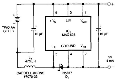
Simple Hot Lead Regulator Circuit Diagram

This Simple Hot-Lead Regulator Circuit Diagram derives 5 Vdc from 2-AA cells—even at their end-life voltages of 1.05 V, and is approximately 80% efficient, providing 5 V at 4 mA from 2.1 V at 11 mA. IC1 is manufactured by Maxim Integrated Products, Inc.


Hot-Lead Regulator Circuit Diagram

Simple Hot-Lead Regulator Circuit Diagram

Here continue read..

THIEF ALARM


BURGLAR ALARM 
 To detect the present robber we have used LDR and a source of light.
LDR is a special type of resistance whose value depends on the brightness of the light which is falling on it. It has a resistance of about 1 megaohms when in total darkness,but a resistance of only about 2-5 k ohms when brightly illuminated. It responds to a large part of the light spectrum.

      The source of light and LDR is so adjusted with a reflector that light will directly fall on the LDR but when robber enters inside then it will block the beam of light and LDR will be under darkness.
1)9V battery with snap                                       
2) LDR
3) Variable resistance 100K ohms
4) Resistance 470 ohms
5) LED
6) IC 555
7) Switch
8) BUZZER

Digital Fan Regulator

The circuit presented here can be used to control the speed of  fans using induction motor. The speed control is nonlinear, i.e. in steps. The current step number is displayed on a 7-segment display. Speed can be varied over a wide range because the circuit can alter the voltage applied to the fan motor from 130V to 230V RMS in a maximum of seven steps.  The triac used in the final stage is fired at different angles to get different voltage outputs by applying short-dura-tion current pulses at its gate. For this pur-pose a UJT relax-ation oscillator is used that outputs sawtooth waveform. This waveform is coupled to the gate of the triac through an optocoupler (MOC3011) that has a triac driver output stage.

Pedestal voltage control is used for varying the firing angle of the triac. The power supply for the relaxation oscillator is derived from the rectified mains via 10-kilo-ohm, 10W series dropping/limit-ing resistor R2.  The pedestal voltage is derived from the non-filtered DC through optocoupler 4N33. The conductivity of the Darlington pair transistors inside this optocoupler is varied for getting the pedestal voltage. For this, the positive sup-ply to the LED inside the optocoupler is connected via different values of resistors using a multiplexer (CD4051).

Digital Fan Regulator Circuit diagram:
Digital Fan Regulator Circuit Diagram

The value of resistance selected by the multiplexer depends upon the control in-put from BCD up-/down-counter CD4510 (IC5), which, in turn, controls forward bi-asing of the transistor inside optocoupler 4N33. The same BCD outputs from IC5 are also connected to the BCD-to-7-seg-ment decoder to display the step number on a 7-segment display.  NAND gates N3 and N4 are config-ured as an astable multivibrator to produce rectangular clock pulses for IC5, while NAND gates N1 and N2 generate the active-low count enable (CE) input using either of push-to-on switches S1 or S2 for count up or count down operation, respectively, of the BCD counter.

Optocoupler 4N33 electrically isolates the high-voltage section and the digital section and thus prevents the user from shock hazard when using switches S1 and S2. BCD-to-7-segment decoder CD4543 is used for driving both common-cathode and common-anode 7-segment displays. If phase input pin 6 is ‘high’ the decoder works as a common-anode decoder, and if phase input pin 6 is ‘low’ it acts as a common-cathode decoder.  Optocoupler 4N33 may still conduct slightly even when the display is zero, i.e. pin 13 (X0, at ground level) is switched  output pin 3. To avoid this problem, adjust preset VR1 as required using a plastic-handled screwdriver to get no output at zero reading in the display.

Source :  http://www.ecircuitslab.com/2011/10/digital-fan-regulator.html


Here continue read..

Sunday, December 22, 2013

Voice Scrambler

With this circuit you can modify how your voice sounds by changing the pitch of your voice. This circuit can be connected to a phone and with a duplicate circuit on the end of the phone line, you can have a scrambled voice communication. The way the circuit works is as follows: If we cut the circuit in half at the T2 transformer and include the LM324 on the left side, you will see that the LM324 portion of the circuit is a tone oscillator which shifts the frequency of all input signals to a new higher frequency.

When the voice and the tone oscillator mix frequencies the voice is not recognized. The voice signal is then inputted to the second stage which again shifts the voice signal again. I recommend that the first stage be tuned to a frequency that is 100hz lower then the second stage.

Here continue read..

Build an Alarm Control Keypad Circuit Diagram

The IC is a quad 2 input “AND” gate, a CMOS 4081. These gatesonly produce a HIGH output, when BOTH the inputs are HIGH. Whenthe key wired to `E` is pressed, current through R1 and D1switches Q5 on. The relay energises; and Q5 is `latched on` byR8. Thus, the Alarm is set by pressing a single key, say one ofthe tw1o non-numeric symbols.The alarm will switch off when the 4 keys connected to“A,B,C,D” are pushed in the right order. The circuit worksbecause each gate `Stands` upon its predecessor.If any key otherthan the correct key is pushed, then gate 1 is knocked out of thestack, and the code entry fails. 

Pin 1 is held high by R4. This`Enables` gate 1; and when button `A` is pressed, theoutput at pin 3 will go high. This output does tw1o jobs.It locksitself `ON` through R2 and it `Enables` gate 2, by taking pin 5,high. Now, if `B` is pressed, the output of gate 2, at pin 4will go high. This output does tw1o jobs. It locks itself `ON`through R3 and it `Enables` gate 3 by taking pin 12 high.Now, if `C` is pressed, the output of gate 3 will lock itself`ON` through R5 and, by taking pin 8 high, `Enable` gate 4.Pressing `D` causes gate 4 to do the same thing; only this timeits output, at pin 10, turns Q4 `ON`. 

This takes the base of Q5to ground, switching it off and letting the relay drop out. Thisswitches the alarm off.Any keys not connected to `A B C D E` are wired to the base ofQ1. Whenever `E` or one of these other keys is pressed, pin 1 istaken low and the circuit is reset. In addition, if `C` or `D`is pressed out of sequence, then Q2 or Q3 will take pin 1 low andthe circuit will reset. Thus nothing happens until `A` ispressed. Then if any key other than `B` is pressed, the circuitwill reset.Similarly, after `B`, if any key other than `C` is pressed,the circuit will reset. The same reasoning also applies to `D`.The Keypad needs to be the kind with a common terminal and aseparate connection to each key. On a 12 key pad, look for 13terminals. The matrix type with 7 terminals will NOT do. 

Wire thecommon to R1 and your chosen code to `A B C D`. Wire `E` to thekey you want to use to switch the alarm on. All the rest go tothe base of Q1.The diagram should give you a rough guide to the layout of thecomponents, if you are using a strip board. The code you choosecan include the non-numeric symbols. In fact, you do not have touse a numeric keypad at all, or you could make your own keypad.I haven`t calculated the number of combinations of codesavailable, but it should be in excess of 10 000 with a 12 keypad; and, after all, any potential intruder will be ignorant ofthe circuit`s limitations. Of Course, if you must have a moresecure code, I can think of no reason why you shouldn`t addanother 4081 and continue the process of enabling subsequentgates. Or you could simply use a bigger keypad with more “WRONG”keys.Any small audio transistors should do. 

The 27k resistors couldbe replaced with values up to 100k. And the only requirementsfor the 4k7 resistors is that they protect the junctions whileproviding enough current to turn the transistors fully on.Capacitors (C1 C2 C3 C4 C5) are there to slow response timeand overcome any contact bounce. They are probably unnecessary.

Alarm Control Keypad Circuit Diagram

Alarm Control Keypad Circuit Diagram

Here continue read..

53 dB Stereo Preamplifier for Tape or Phonographs
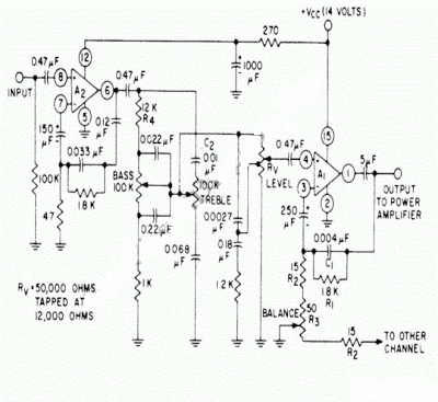
With the circuit shown in the following schematic diagram, both channels of this stereo preamp is constructed using  RCA CA3052 quad AC amplifier.  this pre-amplifier circuit is featured with tone control (bass – treble). Make a similar circuit to complete the other channel, since the circuit for left and right channel are similar. To be high-fidelity, total harmonic distortion should be kept minimum, this circuit gives less than 0.3% distortion level at  at 1-kHz testing signal with 1-V amplitude.  

Gain or amplification at 1 kHz is 47 dB,  and the tone control will curve the response with 11.5-dB boost at 100 Hz and 10 kHz at maximum bass and treble boost.  For minimum bass and treble knob position,  the attenuation will be 10dB  at 100 Hz  and 9dB at 10kHz. This circuit is operated by a single ended supply for wider range environment. Inputs can be from tape recorders pickup or magnetic-cartridge phonographs.

53 dB Stereo Preamplifier for Tape Circuit Diagram


53 dB Stereo Preamplifier for Tape
Here continue read..