Sunday, August 31, 2014

Simple 12 Volt 2 A Switching Power Supply Wiring diagram Schematic

This is a Simple 12 Volt / 2 A Switching Power Supply Circuit Diagram. The schema 12 volt / 2 A switching power supply in the above scheme is not too complicated. At the output of this block provides a stable 12 V and maximum current 2A. Power supply units are quite compact and is suitable for debugging schemes, as well as a permanent resource for stationary devices, including power for the logic electronics for the home-made ​​CNC machine tools. 

12 Volt / 2 A Switching Power Supply Circuit Diagram


12
 
 Transformer is available in the free market and avoids the hassle of having to self-winding. The diode bridge BR 1 of any given voltage and current of 2A. All other elements in the high part of the schema are designed by the same voltage, taking into account the mains. The scheme of 12 volt / 2 A switching power supply operates from the high voltage network, to be observed when mounting accuracy and caution when using. It is desirable to block the finished board to “pack” in the body. 

Sourced By :  powersupply88
Here continue read..

Simple Intelligent Battery Charging Wiring diagram Schematic

 Intelligent Battery-Charging Circuit Diagram . Intended for a Nicad application this charging schema can be used with a wide range of batteries. A low-battery detector is intended. The trip voltage is set via the 500-kQ pot .
Select Rc for the battery you intend to use.

  Intelligent Battery-Charging Circuit Diagram


 intelligent battery-charging circuit diagram
Here continue read..

TDA2003 Car amplifier


This is a very popular series of amplifiers audio users who require maximum aduio results and of course with a relatively cheap price. This circuit requires a minimum voltage and maximum 9 Volt and 30 Volt.
Read more
Here continue read..

Saturday, August 30, 2014

PCBWeb Software

Online CAD system for drawing schemes and creating printed circuit boards of electronic devices.
PCBWeb allows you to draw electrical circuit diagrams, formed on the basis of their circuit boards, export ready-made solutions in the format Gerber, necessary for their manufacture. This application consists of three main parts: Schematic, PCB and Bill of Materials.
At the beginning of the user is a complete list of his projects. You can also create lists of trusted authorized users, who will have the right to open and edit a specific project. In PCBWeb all the features typical of this kind of package, in particular: editing workload (cut, copy, and delete electronic components, undo and redo actions that have occurred), changes in the characteristics of radio components, adding new circuits to an existing project, save and export operations. In addition there are features for configuring ports create multi-circuits and multilayer circuit boards, potting, design rule checking, support for metric and imperial systems of coordinates. With this program you can PCBWeb in real time to generate a list of the components used with the price, and get links to their order.
Software package developed in partnership with Digi-Key , one of the largest distributors of electronic components. Size provided library radioelements really huge, there are a variety of resistance, capacitance, filters, oscillators, generators, inputs, potentiometers, keys, measuring instruments, sensors, batteries, connectors, inductors, memory cards, optoelectronic products, audio components, transformers and much much more. Unfortunately, for many of them there is no graphical display used in the schematic editor and PCB footprint. The program offers to draw them yourself, using the services of the integrated editor.
Among the shortcomings PCBWeb should be noted also that this environment is currently being still in beta testing. The application contains a lot of bugs in the code. As a result - regular and sustained hovering stoppages software. Visually beautiful interface program is not without some shortcomings. Doing some operations are not clear, but the lack of user manual or help file only aggravate the situation. Hopefully, the developers will be able to eliminate all defects and finish the whole ambitious program PCBWeb.
Considered browser application is absolutely free. To get started with the software package PCBWeb need to register on that site, as well as downloading and installing Microsoft Silverlight, allowing to work with Web applications that contain animation and vector graphics.

Developing a program of workers engaged PCBWeb Silicon Frameworks. This organization is located in the small town of Hawi (the northern tip of the island of Hawaii). Silicon Frameworks has strong partnerships in the electronics industry and many years of experience in designing CAD-systems. Currently, the organization is looking for people for the further development of the above online application.
Russian language support no interface software package PCBWeb entirely in English.
The main advantage is the use of PCBWeb software platform Silverlight. Thanks to this application may not work only under Microsoft Windows, but also on Mac and Linux. The only requirement for the end-user hardware is stable and high speed Internet connection.
Considered software is designed to work on PCs running under Microsoft Windows.
Distribution of the program: Freeware
Official site PCBWeb: http://www.pcbweb.com

Here continue read..

14 Watt car audio amplifier circuit

 
Basic operation of this amplifier is on IC TEA2021 ,
In this circuit minimum require voltage is 4 volts and maximum voltage 25 volts. Power output 14 Watt with 4 Ohm impedance. See this schematic.
Here continue read..

DipTrace Software

Automated system through designing electrical circuits and PCB layout.
Simple and easy DipTrace does not require a learning curve and is perfect for small amateur handicrafts. The program consists of the following modules: Schematic (to create a multi-sheet multi-level circuits with built-in simple simulation), PCB Layout (development boards using manual or automatic routing systems and components optimize the location and size of boards), Pattern Editor and Component Editor (to edit buildings and the components, respectively.) DipTrace contains the minimum possible number of controls when working editable objects are highlighted, thus providing an assessment of the situation. Changing one element or circuit board is reflected in all its dependent objects. Autorouter copes with complex multilayer boards that have different types of radio components and support files Specctra DSN / SES lets you connect an outside breeder. The program conducts numerous inspections of the project (new items in the library, affordability and integrity of connections, clearances, dimensions) at various stages of work that can detect and fix errors "on the fly." Creating a SPICE netlist to simulate project allows any external simulator, export / import functions make it possible to continue to work in other applications (P-CAD, PADS, OrCAD, Eagle), as well as use netlists Accel, Mentor, Allegro, Tango and Protel. DipTrace board in exports necessary for the production formats DXF, Gerber RS-274X (with support for TrueType fonts and raster monochrome images), Excellon N / C Drill. Standard library programs include more than 100 000 items from the most reputable manufacturers and convenient development tools allow yourself a few minutes to produce radio parts of any size and complexity. Thanks to a set of three-dimensional models of buildings can be built in the space of the rotating 3D-picture appearance of the final product.


 Since the development of DipTrace programmers engaged in domestic and radio electronics, it is expected that the program itself, textbook, reference materials and other more completely in Russian.DipTrace was created by OOO "Novarm" and distributed in Russia through partner company JSC "Softline".

In addition to the maximum version DipTrace Full, there are versions of Extended, Standard, Lite Starter and different number of available pins, signal layers and, of course, price. To assess the capabilities of the program, you can download a 30-day trial. There is also a crack software, an extensive library of 3D-models of buildings and detailed tutorial from the manufacturer in Russian, which describes step by step all the stages of the development board. In addition, there is a special free version of DipTrace Freeware limited to 300 pins and two layers.

DipTrace operating systems: Linux, Mac OS and Windows NT, 2000, HP, Vista, 7 (32 - and 64 - bit). Manufacturer does not recommend the package to run on Windows 95, 98 and ME. Also, the program does not work in Windows 8, even when activated compatibility mode

Distribution of the program: Freeware (free with limitations) and Shareware (fee required), price - 600 rubles
Official site DipTrace: http://www.diptrace.com/rus


Here continue read..

Friday, August 29, 2014

6x30W Six Channel Class AB Audio Power Amplifier IC

General Description

The STK403-400 series products are audio power amplifier hybrid ICs that consist of optimally designed discrete componet power amplifier circuits that have been miniaturized using Sanyos unique insulated metal substrate technology. The adoption of a newly developed low thermal resisten substrate allows this product to integrate six power amplifier channels in a single compact package.

Circuit Diagram
6x30W Six-Channel Class AB Audio Power Amplifier IC
Datasheet for STK403-400: Download


Here continue read..

TV Remote Control Jammer

This schema confuses the infra-red receiver in a TV. It produces a constant signal that interferes with the signal from a remote control and prevents the TV detecting a channel-change or any other command. This allows you to watch your own program without anyone changing the channel !!    The schema is adjusted to produce a 38kHz signal. The IR diode is called an Infra-red transmitting Diode or IR emitter diode to distinguish it from a receiving diode, called an IR receiver or IR receiving diode. (A Photo diode is a receiving diode).

Circuit

There are so many IR emitters that we cannot put a generic number on the schema to represent the type of diode. Some types include: CY85G, LD271, CQY37N (45¢), INF3850, INF3880, INF3940 (30¢). The current through the IR LED is limited to 100mA by the inclusion of the two 1N4148 diodes, as these form a constant-current arrangement when combined with the transistor and 5R6 resistor.
Here continue read..

Single Cell LED Flashlight

High efficiency white LEDs have advanced to the point where they can replace glow bulbs and other light sources not only as indicators, but also for illumination. While many of the claims made about the LEDs efficiency, light quality, lifetime and economy are mostly exaggeration, the truth is that for very low light levels they are now competitive. They have equal or slightly higher efficiency than a flashlight bulb, a longer lifetime, and are very much tougher. On the other hand, they are still far more expensive than a bulb, for a given light output.

Circuit

It follows that LEDs are almost ideal for very tiny, low power flashlights, in the less-than-one-watt category. But such a low power flashlight makes sense only if the whole flashlight is small and lightweight, and has a reasonable battery lifetime. But white LEDs require about 3.3 volts each, and typically some extra voltage is needed to provide room for current regulation! Thats why most commercial LED flashlights use at least three alkaline or NiMH cells, or a lithium cell. And often they cant use their batteries all the way down to the true end of their charges!

Using three AA cells isnt really practical for a small flashlight, simply because it will no longer be small! Lithium cells are expensive. So some manufacturers use three button cells, but these last only for minutes and are also expensive compared to their tiny energy contents! So I set out to build a schema that lights a string of white LEDs, using a single alkaline or NiMH cell. That allows using the widely available and inexpensive AA cell, obtaining a small size, low cost and good runtime.

A typical white LED has its best power-efficiency combination at about 20mA, and needs about 3.3V. This makes for a power of about 66mW per LED. I decided to use seven LEDs, because they can be arranged in a nice and compact way with one in the middle and the other six around, and the whole array runs at close to one half watt, which is a reasonable power for a tiny pocket flashlight. To avoid having to control the current separately for each LED, the LEDs were arranged in series. So, I needed a driver schema that will provide about 23V at 20mA, when fed from a 1.2V NiMH rechargeable cell  or from a 1.5V alkaline cell. It should be ultra simple, low cost, efficient and reliable. And here it is!

The schema is a self-oscillating boost converter, and I certainly cannot claim having invented it. It is ages old! I only did the detail design of this one, and optimized it in the course of one afternoon. It runs with a beautifully clean waveform, with all components except the LEDs staying completely cold to the touch. At this low power level, even that doesnt guarantee a good efficiency, but I measured it at about 72%, which is quite good for a schema operating from such a low voltage!

How it works:

When switching it on, R1 and D1 bias the transistor into the linear range, through the feedback winding on T1. That causes a current through the 18 turn winding, and thanks to the positive feedback the transistor is driven into saturation. At this moment there will be a base current defined like this: The 1.2V of the cell, plus the 0.2V induced in the feedback winding, minus the 0.7V base-emitter drop of the transistor, make a total of 0.7V, which applied to the 22 ohm resistor gives about 32mA base current. D1 is not conducting a significant current at this time, because the transistor clamps the base voltage to 0.7V and the 3 turn winding subtracts 0.2V from this, so that we end up with only 0.5V across the diode.

This base current keeps the transistor in saturation until its collector current reaches approximately 1A, while the transformer loads up. At this point the transistor will start getting out of saturation, which makes the feedback voltage drop. This very quickly puts the transistor into blockage. The collector voltage will soar as T1 forces current to keep flowing, until D2 starts conducting and discharges the transformer into C2, by means of a quite narrow pulse. During operation this pulse is about 24V high, so that the feedback winding develops -4V, which results in applying about -3.3V to Q1s base, enough to switch it off very fast, but not enough to make the base reverse-conduct.

As soon as the transformer has fully discharged into C2, the voltage on it breaks down, and the transistor enters conduction to start a new cycle. The oscillating frequency is 30kHz, and the transformer operates at a peak flux density of 0.1 tesla, far away from saturation, and low enough to have very low loss. C2 has to eat the load pulses that start at about 1A, and has to keep the voltage constant enough to feed the LEDs an almost smooth DC. The value given works well. If anyone wants to build this schema to run 24 hours a day for 30 years, it would be good to pick a capacitor rated for low ESR and a relatively high ripple current, but for flashlight use a plain standard 47µF, 35V electrolytic capacitor works great.

C1 is not strictly necessary. With a good NiMH cell, the schema works the same without it, so you can save a few cents here. But with the capacitor in place, the schema keeps working better when the cell is almost fully discharged and its internal resistance gets higher, so its better to include it.

Components:

Of course, the part over which most builders will stumble is the transformer. I used an Amidon EA-77-188 core, because I had it at hand, and it was the smallest core I had. I should say that this core is still at least five times larger than required! So feel free to use the smallest ferrite double-E core you can find, or any other ferrite core that offers a closed loop and the possibility of assembling it with an air gap. But then you will have to redo the math!

The main winding has 18 turns, and I wound it with 7 strands of #30 enameled wire twisted together, simply because there is room enough to do so. But this thick wire bundle is huge overkill, like the whole transformer is! The feedback winding  was wound with a single strand of that same #30 wire, and it has just three turns. The phasing is like shown in the diagram, of course. If you get the phasing wrong, the schema wont work and the transistor will get warm.

I used masking tape to hold the windings in place on the bobbin. No special insulation is required, because the voltages are so low that the enamel on the wire is insulation enough.

Now comes a very important step: This transformer is airgapped. The two core halves need to be separated by a distance of 0.1mm. I simply stuck little pieces of masking tape on the three legs of one core half, taking advantage of the fact that my masking tape is just the right thickness! Then I assembled the core, wrapping masking tape around it to hold it together.

If you have to use a different ferrite core, you can use my transformers and coils article to learn how to design your transformer. The turns ratio will of course remain 6:1, but the absolute number of turns will change in inverse proportion  to the cores cross section. You can look up the data of my core on Amidons or Bytemarks websites, compare that to the data for your core, and go from there. After calculating the turns numbers, you have to calculate the required air gap to obtain an inductance of the main winding of about 40µH.

The transistor I used, the 2SC1226A, is a pretty old part and may no longer be available. I have a bunch of them, so I used it. It has a soft, thin copper tab which can easily be cut off, which is an advantage in this schema, because it allows saving some space! The transistor works cold, so it doesnt really need the tab! If you have to use another transistor instead, feel free, but look for one which has the proper characteristics: It should have a breakdown voltage of about 40V, a maximum continuous current of about 3A, be reasonably fast (mine is very fast, having an Ft of 150MHz!), it should have good saturation characteristics, and it should have a reasonably high hfe (at least 30, ideally about 100) at a current of 1A.

Any different transistor will most likely require a change in the value of R1, to set the proper power level for the LEDs. You can experimentally determine that resistor value, by placing a milliamperemeter in series with the LED string, and selecting the resistor for 20mA in the LEDs. By the way, if you want to build this schema for an alkaline cell instead of a NiMH cell, the resistor should be a bit higher. D2 is a Schottky rectifier. A non-Schottky ultrafast diode could be used too, but the Schottky is better. D1 instead is any plain simple silicon diode.

If your power switch doesnt have very low resistance, it might cause a significant loss in this low voltage schema! If that happens, you could instead place the power switch in series with R1, leaving the rest of the schema permanently energized. That will cost almost no lost battery power, because the only current drain when off will be the leakage through the parts, which should be in the microampere range. But if you place the switch at R1, you should also place a 1 megaohm resistor (or almost any other high value) in parallel with D1, to make sure that the transistor really does stay fully off when it should!
Source: Humo Ludens
Here continue read..

TV Remote Control Jammer


This is really fantastic schema.Because you can fun with this schema.If others operate your TV set or setup you can use this to control them.and you can use this to annoy someone.so enjoy with this....


Parts:

Q1 2N4403 PNP Transistor

Q2 2N4401 NPN Transistor

C1 10nF Ceramic Disc Capacitor

C2 1uF Electrolytic Capacitor

D1, D2, D3 High Output IR LED

R1 100K 1/4W Resistor

R2 150K 1/4W Resistor

R3 10K 1/4W Resistor

R4 1K 1/4W Resistor

S1 Normally Open Momentary Push Botton

B1 4.5V Battery (Three "AA"s In Series)

MISC Wire, Case, Board


Note

# You may need to adjust the value of R5 for the right frequency.
#supply 4.5v
Here continue read..

Thursday, August 28, 2014

Battery Saver Wiring diagram Schematic

A small electronic switch that connects a battery to the equipment for a certain amount of time when a push-button is momentarily pressed. And we have also taken the ambient light level into account; when it is dark you won’t be able to read the display so it is only logical to turn the switch off, even if the time delay hasn’t passed yet. The schema is quite straightforward. For the actual switch we’re using a well-known MOSFET, the BS170. A MOSFET (T2 in the schema) used in this configuration doesn’t need a current to make it conduct (just a voltage), which makes the schema very efficient. When the battery is connected to the battery saver schema for the first time, capacitor C2 provides the gate of the MOSFET with a positive voltage, which causes T2 to conduct and hence connect the load (on the 9 V output) to the battery (BT1). C2 is slowly charged up via R3 (i.e. the voltage across C2 increases).

Circuit diagram:


battery-saver-schema-diagramw
Battery Saver Circuit Diagram

This causes the voltage at the gate to drop and eventually it becomes so low that T2 can no longer conduct, removing the supply voltage to the load. In this state the battery saver schema draws a very small current of about 1 µA. If you now press S1, C2 will discharge and the schema returns to its initial state, with a new turn-off delay. Resistor R5 is used to limit the discharge current through the switch to an acceptable level. You only need to hold down the switch for a few hundredths of a second to fully discharge C2. In our prototype, connected between a 9 V battery and a load that drew about 5 mA, the output voltage started to drop after about 26 minutes. After 30 minutes the voltage had dropped to 2.4 V. You should use a good quality capacitor for C2 (one that has a very low leakage current), otherwise you could have to wait a very long time before the switch turns off! 

The ambient light level is detected using an LDR (R1). An LDR is a type of light sensor that reduces in resistance when the light level increases. We recommend that you use an FW150, obtainable from e.g. Conrad as part number 183547-89. When there is too little light its resistance increases and potential divider R1/R2 causes transistor T1 to conduct. T1 then charges up C2 very quickly through R4, which limits the current to a safe level. This stops T2 from conducting and the load is turned off. The choice of value for R2 determines how dark it has to be before T1 starts to conduct. The battery saver schema can be added to devices that use 6 or 9 volt batteries and which don’t draw more than 100 mA. The schema can be built on a piece of experimenter’s board and should be made as compact as possible so that it can be built into the battery powered device.


Copyright : Elektor Electronics
Here continue read..

2 x 75 W Audio Power Amplifier TDA7575

Features:

  • DMOS POWER OUTPUT
  • NON-SWITCHING HI-EFFICIENCY
  • SINGLE-CHANNEL 1Ω DRIVING CAPABILITY
  • HIGH OUTPUT POWER CAPABILITY 2x28W/
  • 4Ω @ 14.4V, 1KHZ, 10% THD, 2x40W/4Ω EIAJ
  • MAX. OUTPUT POWER 2x75W/2Ω, 1x150W/1Ω
  • SINGLE-CHANNEL 1Ω DRIVING CAPABILITY
  • 84W UNDISTORTED POWER
  • FULL I2C BUS DRIVING WITH 4 ADDRESS
  • ST-BY, PLAY/MUTE, GAIN 12/26dB, FULL
  • DIGITAL DIAGNOSTIC
  • POSSIBILITY TO DISABLE THE I2C
  • DIFFERENTAL INPUTS
  • FULL FAULT PROTECTION
  • DC OFFSET DETECTION
  • TWO INDEPENDENT SHORT CIRCUIT 
  • CLIPPING DETECTOR PIN WITH SELECTABLE THRESHOLD (2%/10%)
  • ST-BY/MUTE PINS
Block Diagram:
Block Diagram

Here continue read..

1959 Chevrolet Passenger Wiring Diagram

1959 Chevrolet Passenger Wiring Diagram
The part of 1959 Chevrolet Passenger Wiring Diagram: license lamp, backup lamp, dimmer switch, starter solenoid, spark plugs & distributor, clock lamp, cigarette lighter, neutral safety & backup switch.
Here continue read..

Wednesday, August 27, 2014

Voltage Monitor Wiring diagram Schematic

This is a very simple schema which can be modified to the users needs. Its operation is simple, when the input voltage is 0, the LED (LO). The LED turns off when the voltage increases to the level determined by R2.


Voltage Monitor Circuit Diagram

Voltage

Here continue read..

Wednesday, August 13, 2014

PCB Exposure Switch Timer V2 0

After some modifications on my UV exposure box (scanner) for better UV expose, i decided that a better pcb must me designed for switch timer. The old one had over drilled holes and it was designed and built on my very fist steps. Also the high voltage side from the low voltage wasn’t separated as it needed to be safe.
PCB Exposure Switch Timer V2.0

So i redesigned it in a more compact and easier to use pcb. The firmware has been also updated and now you can program the timmer by using the two buttons. The time is calculated by timer interrupt triggering using a 32.768KHz RTC Crystal with better accuracy. The display update also has been changed from static to dynamic. [Link]
Here continue read..

Tuesday, August 5, 2014

Build a Cell Phone Jammer Schematic Diagram

Build a Cell Phone Jammer Schematic Diagram
 
This cell phone jammer operates at GSM800 frequency since most mobile phones use it to operate. So the selected VCO is a sweeping oscillator, which is very effective but may be hard to construct for the beginners without nice RF-testing equipment.

As a noise source you can use 45MHz clock oscillator which is driving Local Oscillator port located on a mini-circuit mixer. There is also an impedance matching network for Local Oscillator signal to pass through it. It is used to equate impedances of the clock oscillator and the port of the mixer.

RF input (which is this port of the mixer) connected to the first 800MHz cell phone antenna, and the RF output is sent to the mini-circuit amplifier. This amplifier increases the output power for 15-16dbm. The amplified signal then sent to the second cell phone antenna.

Build a Cell Phone Jammer Schematic Diagram


 works
All cell phones which use GSM800 have their transmitted and received frequencies always separated by 45MHz. So when the mobile phone tries to call it is blocked by its own signal returning to it! Isn’t that cool? When the phone blabber annoys you – turn your jammer on and that wrongdoer will hear own voice in his or her cell phone.

Oh, by the way, you can also use this mobile signal jammer to block any cell-based tracking systems which use your GPS to track and record your car’s moves. And it is quite possible (though I didn’t actually tested it) to jam IEDs which detonated using cell phones.

Build a Cell Phone Jammer Schematic Diagram


The mixer used is designed to work up to 600MHz but in this case it works pretty well.

Build a Cell Phone Jammer Schematic Diagram
 
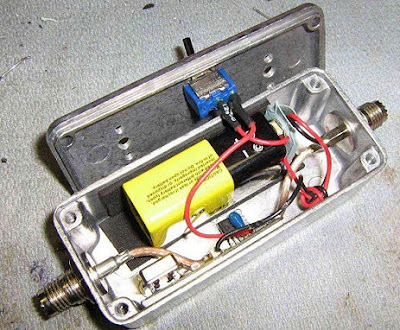
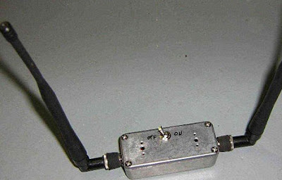
RF amplifier is doing its job perfectly yet (as it was mentioned in the Jammer Store blog post) draws additional power.Old aluminium box was used as a frame for the jammer and old UHF connectors from Motorola cell phone as input/output.You need to attach RF connectors to the circuit. Nine volt battery and voltage regulator were used to supply all components. The battery was placed inside and separated by the foamed plastic from the other components.The power on/off switch is placed on the top. The input and output antennas (also from old Motorola mobile phone) are screwed onto UHF connectors.Your cell phone jammer is ready. Enjoy!

Build a Cell Phone Jammer Schematic Diagram


Here continue read..