Friday, October 31, 2014

Power Amplifier MJ15003 MJ15004 c200


The c200 is the result of numerous diyers request for a basic discrete power amplifier. As such, this amplifier is specially designed to meet the following: fairly high power output. easy to construct. use common components. no oscillations. have current limit protection. above average hifi performance. bridgeable for HT subs. rugged enough for party use. Power Output Output of the c200 into 8 ohms before clip is 125 Watts. When loaded to 4 ohms, the output is increased to 200 Watts. With 2 channels operating in bridged mode, power output is a respectable 400 watts into 8 ohms. Output Transistors For easy procurement, very common transistors have been chosen for the c200. The power transistors comprise of 4 pieces of MJ15003 and MJ15004. Though "slow" (fT=2MHz) by todays standards, these transistors are easily available, reasonably priced, has sufficient power rating and the necessary SOA for audio. For those who prefer to use 2N3055 and MJ2955, the c70 model, with 70 Watts/RMS output is available. Vas & Drivers TIP29C/30C are used for these stages. Though equally slow (fT=3MHz), they are chosen based on availability and cost. Input Differential 2N5551 is used for input. Again, this is a common part number with properties suitable for audio.


THD Testing

Before we proceed with power testing, substitute the dummy load with a 200 watts, 8 ohms resistor. With the probes of the THD analyzer connected across the load, spot frequencies of 200Hz, 1KHz, 10KHz and 20KHz are used to test the amplifiers THD at 1Watt, 60Watts and its rated output of 125Watts. You should be able to record similar readings as in Fig 5. It is recommended that the power heatsink and dummy load be suitably cooled to avoid overheating. For 4 ohms testing, replace load with a 400 watts resistor.


Fig 5 - THD + N


Note that as you gradually increase the output to maximum level, the output waveform should not exhibit any signs of distortion until clip.


The Power Supply Unit (PSU)

The PSU (Fig 9) is a conventional, unregulated supply. Input fuse F1 is for safety. Mains switch SW1, has its contacts straddled by a 4700pF X2 capacitor to suppress "popping" during switch-on. T1 is the power transformer with a secondary output of 40-0-40Vac. BR1 is the bridge rectifier and C2,C3 are the filter capacitors for DC smoothing. Power Supply Unit For monoblock, C2,C3 = 10,000uF x2/63V minimum. Transformer secondary should be rated for 250VA. For stereo, C2,C3 = 22,000uF x2/63V minimum. Transformer should be upgraded to 500VA. Supply rails (Vs) are +-53Vdc.


The c300 up close
This 300 Watts/RMS amplifier is meant for those who are not only looking for higher power, but superior performance as well. In order to achieve this, the c300 features some advanced techniques that are absent in its smaller counterpart (c200).


Additions in 1st Gain Stage

Cascodes
Right at the very first gain stage, cascodes (Q5,6) are adopted. They serve to improve the high frequency performance of the c300. These cascodes are biased to approximately midpoint between 0V and +V by zener diode D1 (33V).

Current Mirrors
The first stage also contains current mirror Q3,4. As the name implies, the mirror forces equal current in the LTP (long tail pair). It is known for its active loading and high gain properties.

Emitter Degeneration Resistors
Slew rate of the input differential is improved by resistors R6,7,8,9,10. In the absence of matched transistors, preset R10, is used for trimming DC to a minimum at the output of the amplifier.


Buffering the 2nd Stage

The VAS mod
The 2nd stage is direct coupled to the differential via a darlington Q8. This effectively buffers Q10, the main transistor that is amplifying the voltage from loading the preceding stage. Q10 is biased into class A by constant current source Q12. Capacitor C9 sets the dominant pole in Miller compensation.


Thermal Tracking

The remaining parts of the circuit is conventional. Vbe multiplier Q11, adjust the bias for the output transistors which is in full complementary EF configuration. Q11 must be thermally coupled to the main power heatsink for proper thermal tracking. VI Limiting network consists of Q13,14, R25~30 and D3,4. This network is optional, and can be omitted if desired.


THD of c300


Biasing of output transistors
All THD readings were done with outputs biased to 20mV across 0.39 ohms emitter resistor. This works out to approximately 55mA per output transistor in idling state.
Here continue read..

Digital Step Km Counter Circuit Diagram

This circuit measures the distance covered during a walk. Hardware is located in a small box slipped in pants pocket and the display is conceived in the following manner: the leftmost display D2 (the most significant digit) shows 0 to 9 Km. and its dot is always on to separate Km. from hm. The rightmost display D1 (the least significant digit) shows hundreds meters and its dot illuminates after every 50 meters of walking. A beeper (excludable), signals each count unit, occurring every two steps. A normal step was calculated to span around 78 centimeters, thus the LED signaling 50 meters illuminates after 64 steps (or 32 operations of the mercury switch), the display indicates 100 meters after 128 steps and so on.

For low battery consumption the display illuminates only on request, pushing on P2. Accidental reset of the counters is avoided because to reset the circuit both pushbuttons must be operated together. Obviously, this is not a precision meter, but its approximation degree was found good for this kind of device. In any case, the most critical thing to do is the correct placement of the mercury switch inside of the box and the setting of its sloping degree.

Digital Step-Km Counter Circuit diagram:


digital_step_km_counter_circuit_diagram
Digital Step-Km Counter Circuit Diagram


Parts:
R1 = 22K 1/4W Resistor
R2 = 2.2M 1/4W Resistor
R3 = 22K 1/4W Resistor
R4 = 1M 1/4W Resistor
R5 = 4.7K 1/4W Resistor
R6 = 47R 1/4W Resistor
R7 = 4.7K 1/4W Resistor
R8 = 4.7K 1/4W Resistor
R9 = 1K 1/4W Resistor
C1 = 47nF 63V Polyester Capacitor
C2 = 100nF 63V Polyester Capacitor
C3 = 10nF 63V Polyester Capacitor
C4 = 10µF 25V Electrolytic Capacitor
D1 = Common-cathode 7-segment LED mini-display (Hundreds meters)
D2 = Common-cathode 7-segment LED mini-display (Kilometers)
Q1 = BC327 45V 800mA PNP Transistors
Q2 = BC327 45V 800mA PNP Transistors
P1 = SPST Pushbutton (Reset)
P2 = SPST Pushbutton (Display)
IC1 = 4093 Quad 2 input Schmitt NAND Gate IC
IC2 = 4024 7 stage ripple counter IC
IC3 = 4026 Decade counter with decoded 7-segment display outputs IC
IC4 = 4026 Decade counter with decoded 7-segment display outputs IC
SW1 = SPST Mercury Switch, called also Tilt Switch
SW2 = SPST Slider Switch (Sound on-off)
SW3 = SPST Slider Switch (Power on-off)
BZ = Piezo sounder
B1 = 3V Battery (2 AA 1.5V Cells in series)

Circuit operation:

IC 1A & IC 1B form a monostable multi vibrator providing some degree of freedom from excessive bouncing of the mercury switch. Therefore a clean square pulse enters IC2 that divides by 64. Q2 drives the LED dot-segment of D1 every 32 pulses counted by IC2. Either IC3 & IC4 divide by 10 and drive the displays. P1 resets the counters and P2 enables the displays. IC1C generates an audio frequency square wave that is enabled for a short time at each monostable count. Q1 drives the piezo sounder and SW2 allows disabling the beep.

Notes:
  • Experiment with placement and sloping degree of mercury switch inside the box: this is very critical.
  • Try to obtain a pulse every two walking steps. Listening to the beeper is extremely useful during setup.
  • Trim R6 value to change beeper sound power.
  • Push P1 and P2 to reset.
  • This circuit is primarily intended for walking purposes. For jogging, further great care must be used with mercury switch placement to avoid undesired counts.
  • When the display is disabled current consumption is negligible, therefore SW3 can be omitted.
Here continue read..

Tri Waveform Generator Circuit Diagram

This is the simple Tri-Waveform Generator Circuit Diagram. The Tri-Waveform Generator can be used for a number of different uses. The one that I use it for is a signal generator to test circuits. The frequency range is 20 to 20khz. and can be adjusted by R1. The duty cycle or the time that the waveform is high and the time that the waveform is low can be adjusted by R4. The purpose of R2 and R3 are to clean up any distortion on the sine wave output. To do this you must hook up the sine wave output to and oscilloscope and adjust R2 & R3 to make the sine wave as accurate as possible.

Here continue read..

Thursday, October 30, 2014

800W high power mosfet amplifier

This amplifier can be used for practically any application that requires high power, low noise, distortion and excellent sound. Examples would be Sub-woofer amp, FOH stage amplifier, One channel of a very high-powered surround sound amplifier etc.

800W

For detail explanation about how this circuit works include the large schematic diagram, power supply schematic diagram and complete component listing, link download this complete article.
Here continue read..

Wiring diagram Volvo S40 Download

Wiring diagram Volvo S40 Download Sensors for pressure in the intake manifold links coil wiring. Airconditioning links 30 85 86 87 relay Bosch 0332 014 112 or equiv 12V air compressor control of compressor S40 PIN 11 ground signal power on Earth. Running a sensor on the left is Oscilloscope projection of good pure signal of magnetic sensor for running 36-1 wheel.


here Wiring diagram Volvo S40 Download

Here continue read..

Electric Stable USB Power Supply Circuit Diagram

This is an Electric Stable USB Power Supply Circuit Diagram. A common problem when an AC mains adapter is used to power a USB device is that the voltage does not match the nominal 5 V specified by the USB standard. The circuit shown here accepts an input voltage in the range of 4-9 V and converts it into a 6-V output voltage, which is then stabilized to a clean 5-V level by a series regulator. The combined boost/buck converter used here operates on the SEPIC principle. That principle is quite similar to the operating principle of the Cuk converter, but without the disadvantage of a negative output voltage.

Stable USB Power Supply Circuit diagram :

Stable-USB-Power-Supply-Circuit-Diagram

Stable USB Power Supply Circuit Diagram

The circuit is built around a MAX668, which is intended to be used as a controller for boost converters. The difference between a SEPIC converter and a standard boost (step-up) converter is that the former type has an additional capacitor (in this case C2) and a second inductor (in this case, the secondary winding of transformer L1). If C2 is replaced by a wire bridge and the secondary winding of L1 is left open, the result is a normal boost converter. In that case, a current can always flow from the input to the output via L1 and D1, even when the FET is not driven by IC1. Under these conditions, the output voltage can never be less than the input voltage less the voltage drop across the diode.

The operation of a SEPIC converter can be explained in simple terms by saying that C2 prevents any DC voltage on the input from appearing at the output, so the output voltage can easily be made lower than the input voltage. The second coil causes a defined voltage to be present at the anode of D1. It is also possible to replace the transformer by two separate coils that are not magnetically coupled. However, the efficiency of the circuit is somewhat higher if coupled coils are used as shown here. The value of resistor R4 is chosen to limit the maximum current to 500mA, which is also the maximum current that a USB bus can provide according to the specifications. Resistors R1 and R2 cause the voltage across C3 and C7 to be regulated at a value of around 6 V. A low-drop regulator (LM2940) is used to generate a stabilized 5V from the 6V output (with ripple voltage). The efficiency should be somewhere between 60% and 80%
Here continue read..

Low Output Power Amplifier


This Low Output Power circuit was a presented,it can go power output around 1 Watt, whilst connected to a power supply 9 volt. The pro of this Low Output Power Amplifier is with the purpose of it uses a dual dear ton to enhance the size at the same time as much as of input impedance about 20 Meg ohm. This circuit unlike other circuits,the input impedance is a constant about 20 Meg ohm each time, whether to adjust the volume control on several level.

Low
Low Output Power Amplifier Diagram Schematic
The components participating in the circuit, it is tightfisted, especially the BC549 transistor output amount after the increase force be present very distorted, it have got to reduce the current level to a safe By dipping the volume down. The sector output in place of the R1 and C1 in order to reduce the oscillator profit is, the truth to the output sector, with an op-amp acts drive dual complementary.
Here continue read..

Wednesday, October 29, 2014

Advance High Voltage Stun Gun Circuit Diagram


This is an Advance High Voltage Stun Gun Circuit Diagram, This device produces high voltage pulses discrupting muscles and nervous sYstem, leaving anyone who touches it in a state of menthal confusion. Can be used agains ferocious animals or attackers, BUT REMEMBER, this device may be illegal in your state (for eg where I live, these devices are banned). It is quite dangerous for peoples experiencing cardiac problems, and for electronic equipment (like peacemakers), since it generates some RF. Dont attept irresponsible actions with this device, it is not a toy.

 Advance High Voltage Stun Gun Circuit Diagram


Advance


After the introduction lets pass to the circuit.

The 555 IC is wired as a astable to produce square wave with adjustable freq and duty cycle (notice the potentiometers and diode). This square wave is feed to a IRF840 Mosfet (no need of totem transistors since freq is low and the IC has enough current capability to rapidly charge/discharge the gate). As a substitute of the mosfet, a bipolar transistor can be used (and a 100ohm resistor between 555 and base of the transistor). Valid BJT can be BU406, but also smaller BJT can be ok, keep in mind that it must handle at least 2A continuous. The inductive kick snubber isnt needed because the power is low and it is almost totally adsorbed to charge the tank capacitor, in addition since this device is battery operated we dont want to dissipate the power on a resistor but we want it in sparks. With a snubbing network you will experience lower firing rates. 
USE A PUSHBUTTON SWITCH FOR SAFETY
Construction of T2: this is the real boring part. Since it is unlikely to find it in shops we need to build them. Materials needed: enamel copper wire (0,20 mm or 0,125 mm), ferrite stick, LDPE sheets (0,25 mm). Secure the ferrite stick with a layer of ldpe (polyethilene, as a substiture use electric insulating tape) and glue it (or tape it) Place 200-250 windings on the ldpe (even more windings if the stick is more than 1), another ldpe layer, another 200-250 windings and so on to finally have 5-6 layers (approx 1000-1400 turns but even more doesnt hurt performance, but be careful for internar arcing that will ruin it). Insulate it again and place the primary winding, 15-20 turns of 1mm wire are just ok, too much windings (too mush resistance and inductance) will lead to smaller current and smaller spike in T2 secondary because of lower rise time,and too few will not saturate the core. I chosen MKP capacitors because they have low ESR and ESL (they are widely used in tesla coils as mmc capacitors).

The spark gap can be simple two crossed (but not touching) 1 mm spaced wires. It acts as a voltage controlled switch, firing when the voltage is enough to ionize the air between them (turning it to plasma with small resistance). Keep in mind that it would be wise do place it into a small plastic container and fill with oil letting bubbles out (dont use motor oir or frying oil but pure mineral oil which has no water in it.

Author:Jonathan Filippi, jonathan.filippi@virgilio.it
Here continue read..

Mic Audio Amplifier Circuit Diagram

The compact, low-cost condenser mic audio amplifier described here provides good-quality audio of 0.5 watts at 4.5 volts. It can be used as part of intercoms, walkie-talkies, low-power transmitters, and packet radio receivers. Transistors T1 and T2 form the mic preamplifier. 

Resistor R1 provides the necessary bias for the condenser mic while preset VR1 functions as gain control for varying its gain. In order to increase the audio power, the low-level audio output from the preamplifier stage is coupled via coupling capacitor C7 to the audio power amplifier built around BEL1895 IC.BEL1895 is a monolithic audio power amplifier IC designed specifically for sensitive AM radio applications that delivers 1 watt into 4 ohms at 6V power supply voltage. 

It exhibits low distortion and noise and operates over 3V-9V supply voltage, which makes it ideal for battery operation. A turn-on pop reduction circuit prevents thud when the power supply is switched on. Coupling capacitor C7 determines low-frequency response of the amplifier. Capacitor C9 acts as the ripple-rejection filter.

Mic Audio Amplifier Circuit Diagram
.
Condenser
Condenser Mic Audio Amplifier Circuit Diagram

Capacitor C13 couples the output available at pin 1 to the loudspeaker. R15-C13 combination acts as the damping circuit for output oscillations. Capacitor C12 provides the boot strapping function. This circuit is suitable for low-power HAM radio transmitters to supply the necessary audio power for modulation. With simple modifications it can also be used in intercom circuits.


Author: D. Prabakaran - Copyright: Electronics For You Mag
Here continue read..

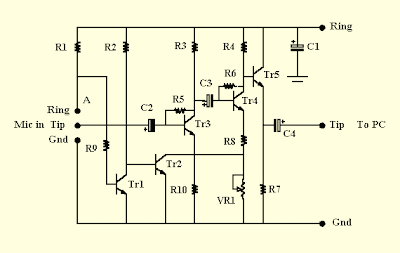
Dual Mode Microphone Pre Amplifier

This is a microphone pre-amp which I designed intended for function with a SoundBlaster(TM) AWE 64 charge sound license; but it be supposed to exist apt for one compatible tag otherwise PC audio input which provides a 5 Volt supply (via a 2k2, or else thereabouts, built-taking part in current-limiting resistor) by the side of the ring call of a stereo jack plug inserted into the "Mic In" socket of the license/PC. (N.b. it has lone been tested with the AWE 64 certificate.)

The circuit has the following skin tone :
(1) It wish without human intervention detect whether a mike plugged into it is of the electret (condenser) otherwise dynamic type and will switch sandwiched between respective "low-addition" and "far above the ground-gain" modes accordingly. The van-detection relies on help of a stereo plug fitted to an electret mike and use of a mono plug fitted to a dynamic mike.
(2) It is powered just by the 5 Volt existing next to the "Mic in the field of" socket.
(3) It is trivial adequate to happen housed in a standard plastic 35mm film flask (remember folks?).
(4) A trimmer allows the next of kin win intended for the two microphone types to be adjusted.
(5) The gain is sufficient to award something like 60mV summit-to-peak next to the "Mic In" socket, obligatory for complete recording level at home WaveStudio.
(6) In conjunction with the licenses built-in input amplifier, the circuit provides a lifeless frequency response done the audio range, with -3dB points on <10 hz and 19 khz.
(7) Input impedance > 10k. Output impedance <1k

Dual-Mode

Component Values :
R1 = R7 = 4k7; R2 = R3 = 47k; R4 = 39k; R5 = R6 = 100k; R8 = 220; R9 = 10k; R10 = 2k2 (all 1/8 Watt). VR1 = 10k
horizontal pre-set. C1 = 47uF; C2 = C3 = C4 = 10uF (all 10V or greater, miniature radial electrolytics). Tr1 = Tr2 = Tr3 = Tr4 = Tr5 = BC108, BC184, BC547, ZTX337 or similar low-power (preferably low noise) NPN transistor
Here continue read..

Tuesday, October 28, 2014

TRANSISTOR TESTER 1

TRANSISTOR TESTER - 1

Transistor Tester - 1 project will test all types of transistors including Darlington and power. The circuit is set to test NPN types. To test PNP types, connect the 9v battery around the other way at points A and B.

10mH choke with 150 turns for the secondary


The transformer in the photo is a 10mH choke with 150 turns of 0.01mm wire wound over the 10mH winding. The two original pins (with the red and black leads) go to the primary winding and the fine wires are called the Sec.

Connect the transformer either way in the circuit and if it does not work, reverse either the primary or secondary (but not both).

Almost any transformer will work and any speaker will be suitable.

If you use the speaker transformer described in the Home Made Speaker Transformer article, use one-side of the primary.
 
 
TRANSISTOR TESTER-1


CIRCUIT
Here continue read..

TA8122 bassed AM FM radio receiver Diagram


A very simple low power AM FM radio receiver electronic projects can be designed using the TA8122 integrated AM FM receiver , manufactured by Toshiba Semiconductor . This radio receiver circuit can be used for portable radio applications or other similar devices .

TA8122 radio receiver circuit supports a wide input voltage range from 1.7 volt up to 7 volts , but for this AM FM radio receiver circuit we will need just a 3 volt DC input voltage ( you can use two 1.5 volt Batteries ) .

Using this receiver integrated circuit you can design a very simple AM FM radio receiver or a radio receiver circuit that supports just one of this band (AM or FM) using few additional components .

Here continue read..

Quadraphonic Amplifiers

This is a four channel amplifier ideally suited in place of utilization with quadraphonic equipment such like a Sound Blaster Live tag. present is rejection volume control,audio levels being in a straight line controlled from the sound tag itself.

Quadraphonic

Component Parts :
D1-D4: 1N4001 (4) 
C1,C20: 1000u CAP (2) 
C2,C11: 47u CAP (2) 
C3,C5,C7,C8,C12,C14,C16,C17,C21,C22: 0.1u CAP (10) 
C4,C6,C13,C15: 10u CAP (4) 
C9,C10,C18,C19: 2200u CAP (4) 
R1,R4,R9,R12: 1M RESISTOR (4) 
R2,R6,R10,R14: 100k RESISTOR (4) 
R3,R5,R11,R13: 1k RESISTOR (4) 
R7,R8,R15,R16: 2R7 RESISTOR (4) 
IC1: 7812 (1) 
IC2,IC3: LM1778N (2) 
SPK1,SPK2,SPK3,SPK4: 8R 2 Watt speakers (4) 

Clarification:
Construction is straight cheeky and is apposite in favor of Verobaord. Overall collect is controlled by the ratio R14/R13 and R6/R5. Used with minor hifi speakers the volume was too loud for my extent so I cut-rate R14 and R6 to 33k. The zobel net formed by R7,C7,R8,C8,R15,C16,R16,C17 prevents instability which can take place with slow spokesperson wires. The input impedance is summit, 1M and if very long input cables are award can pick up sound. Screened cable must come about used, now my folder I used 10k resistors among points A & C, B & C, D & F, E & F. This provides a DC path to ground and top clamor exemption. If instability does occur, at that moment you desire notice sound distortion and the LM1877N will develop into passionate to bit.
associates:
The back of a sound blaster live certificate has colour oblique 3.5mm stereo jacks. The image lower shows a close up of the rear of my Sound Blaster Live tag. in the function of well as colour coding, every connector has an appropriate marking, intended for laid-back connectivity.

The customary output connector is conservational and the rear narrator connector is black. Creative provide utilities and sound mixer for exercise with Windows. Under Linux the helpfulness Gamix can remain used, which allows autonomous volume control instead of all channels.


Here continue read..

Simple condenser microphone circuit

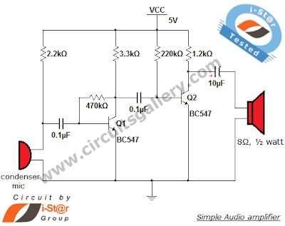
This is a very use full and simple circuit diagram for amplifying weak signal from a capacitive condenser microphone. You can use this circuit for sound sensing applications and some automatic robotic sensors. We have already posted an Efficient audio amplifier circuit using 1895 IC; it is somewhat complicated and suitable for very sensitive applications. But this condenser microphone DIY audio sound amplifier is very small and simple to implement because it uses only two BC547 transistors and some discrete components. You can construct this circuit with minimum of $2 price. This circuit apt for cheap amplification purposes in electronics such as pre amplifier for FM Transmitter.
Circuit diagram


Components required
    Resistors (2.2kΩ; 3.3kΩ; 470kΩ; 220kΩ; 1.2kΩ)
    Capacitors (0.1µF x 2; 10µF,16V)
    Transistors (BC547 x 2)
    Condenser mic
    Speaker (8Ω, ½ Watt)

Working mini audio amplifier 
The circuit is alienated into three divisions: Condenser mic, Audio amplifier and loudspeaker.
    Condenser mic is a type of capacitive audio sensor (audio transducer) that converts the sound (audio) signal into electrical signals.
    These electrical signals are too weak so it is amplified by the amplifier unit. The amplified output is obtained across the speaker.
    The output of condenser mic is coupled via a coupling capacitor of 0.1µF, the purpose of this capacitor is to remove DC contents in the audio signal.
    A 2.2kΩ resistor is used to give the required biasing to the condenser microphone.
    Transistor Q1 is configured as collector to base biasing mode. This is accomplished via 470kΩ resistance. This resistor provides negative feedback to the transistor Q1.
    The output of Q1 becomes available at the collector (across 3.3kΩ resistor), which is the input to the transistor Q2 via a 0.1µF capacitor. The capacitor removes DC voltages due to the biasing of Q1.
    Transistor Q2 is configured as fixed bias using 220kΩ resistor. It also provides further amplification.
    The amplified output from Q2 is available across the 1.2kΩ resistor.
    The 10µF electrolytic capacitor also used to block the DC voltages associated with the biasing of transistor Q2.
    Use 8Ω, ½ watt speaker to hear the amplified signal.
Here continue read..

Monday, October 27, 2014

X Ray Protector Circuits

A protector system that is applied at the beginning of the television technique, therefore most often found on old aircraft models. If the high voltage anode of the picture tube flyback tranfo exceed the permitted limit, the picture tube can generate x-rays from the anode and shadowmask are bombarded by electrons at high speed. To avoid this problem then mounted x-ray surge protector circuit , which automatically "horizontal section will be turned off" if the high voltage from the flyback over.

X-Ray vertical protect

The workings of x-ray protector:

  • High voltage flyback sampled (generally taken from the pin-heater), rectified and is derived using a divider (devider) that uses a resistor-type high-precision resistor. Sample voltage is used to determine whether the condition is normal flyback voltage or over.
  • A "zener diode" as a voltage sensor connected to the sample. In normal conditions the amount of the sample voltage is below the zener voltage of diode so that the condition "off" or is not transparent.
  • Suppose there is a sudden event increased flyback voltage - the voltage will rise above the sample diode voltage value, which causes the diode "on" or voltage through the diode, which would trigger protectionist active work.


Problems that can lead to x-ray active protector works:

  • Damage that causes the power supply voltage B + or incorrect adjustment over
  • Resonant capacitor to the collector of transistor HOT off the decline or solder
  • Tranfo replacement flyback mounted do not match.
  • Damage to one part in the sensor circuit protectors x-ray alone


X-ray Protect Circuit


Here continue read..

200W Stereo High Power Amplifier LM3886

This audio amplifier designed uses two LM3886 per channel, in parallel circuit, based on the PA100 parallel amplifier detailed in National Semiconductors application note - AN1192. This amplifier can deliver about 50W into a 8-ohm speaker and 100W into a 4-ohm speaker. This is a stereo amplifier and therefore 4 LM3886s are used.

The LM3886 circuit is in a non-inverted configuration, so the input impedance is determined by the input resistor R1, i.e. 47k. The 680 ohm and 470pF resistor capacitor filter network is used to filter out the high frequency noise at the RCA input. The 220pF C4 and C8 capacitors are used to shot out the high frequency noise at the LM3886 input pins.

I used high quality audio grade capacitors at several locations: 1uF Auricap at the input for DC blocking, 100uF Blackgate for C2 and C6, and 1000uF Blackgate at the supply filter.
LM3886 Power Amplifier Schematics

The PCB is designed in a way that the power ground is separated from the signal ground, as you can see from the below layout. The signal ground is located in the middle and surrounded by the power ground. There is a thin trace near C5 connecting them. The PCB layout is done by using PADS PowerPCB 5.0. I think it is a powerful layout software.

Amplifier Printed Circuit Board (PCB)
Amplifier Printed Circuit Board Bottom

Amplifier Printed Circuit Board Top
Amplifier Printed Circuit Board
Amplifier Power Supply
The power supply used is a regulated power supply. I used 10000uF per rail before the LT1083 regulator. After the regulator, I have 100uF on the regulator board. The advantage of using regulator is that the power supply ripple voltage is removed. If power regulation is not used, I can hear very little 50/100Hz hum from the speaker.

The high current MUR860 diode is used to ensure high current flow. The voltage regulator used is LT1083, it can provide about 8A of current. Transformer used here is a 500VA 2x 25V. The power supply is then regulated by 2 LT1083, after the regulation, the voltage is 30V.
Power Supply Recomended
I did some DC measurement and the result is quite good, I got 7 mV of DC offset at the speaker terminal. The voltage difference between the output of the 2 chips is less then 1 mV.

The sound of this amplifier is similar to my LM3875 amplifier, which is very clean and detail. It has no hum, no hiss and no noise. Compared to the LM3875 Gainclone, this amp can deliver twice the power to my 4-ohm speaker, and it improves the dynamics and bass punch a lot.
Here continue read..

Very Simple Bench Amplifier Diagram Circuit

A small 325mW amplifier with a voltage gain of 200 that can be used as a bench amplifier, signal tracer or used to amplify the output from personal radios, etc. The circuit is based on the National Semiconductor LM386 amplifier. In the diagram above, the LM386 forms a complete non-inverting amplifier with voltage gain of x200. A datasheet in PDF format can be downloaded from the National Semiconductor website. The IC is available in an 8 pin DIL package and several versions are available; the LM386N-1 which has 325mW output into an 8 ohm load, the Lm386N-3 which has 700mW output and the LM386N-4 which offers 1000mW output. all versions work in this circuit. The gain of the Lm386 can be controlled by the capacitor across pins 1 and 8. With the 10u cap shown above, voltage gain is 200, omitting this capacitor and the gain of the amplifier is 20.

Finished project:
Circuit diagram:
Bench Amplifier Circuit Diagram

The IC works from 4 to 12Volts DC, 12Volt being the maximum recommended value. The internal input impedance of the amplifier is 50K, this is shunted with a 22k log potentiometer so input impedance in this circuit will be lower at about 15k. The input is DC coupled so care must be taken not to amplify any DC from the preceeding circuit, otherwise the loudspeaker may be damaged. A coupling capacitor may included in series with the 22k control to prevent this from happening.
Here continue read..

Sunday, October 26, 2014

Playback Amplifier For Cassette Deck

For some time now, there have been a number of tape cassette decks available at low prices from mail order businesses and electronics retailers. Such decks do not contain any electronics, of course. It is not easy to build a recording amplifier and the fairly complex magnetic biasing circuits, but a playback amplifier is not too difficult as the present one shows. The stereo circuits in the diagram, in conjunction with a suitable deck, form a good-quality cassette player. The distortion and frequency range (up to 23 kHz) are up to good standards. Moreover, the circuit can be built on a small board for incorporation with the deck in a suitable enclosure. Both terminals of coupling capacitor C1 are at ground potential when the amplifier is switched on.

Circuit diagram:Cassette
Cassette Deck Playback Amplifier Circuit Diagram

Because of the symmetrical ±12 V supply lines, the capacitor will not be charged. If a single supply is used, the initial surge when the capacitor is being charged causes a loud click in the loudspeaker and, worse, magnetizes the tape. The playback head provides an audio signal at a level of 200–500 mV. The two amplifiers raise this to line level, not linearly, but in accordance with the RIAA equalization characteristic for tape recorders. Broadly speaking, this characteristic divides the frequency range into three bands:
  • Up to 50 Hz, corresponding to a time constant of 3.18 ms, the signal is highly and linearly amplified.
  • Between 50 Hz and 1.326 kHz, corresponding to a time constant of 120 µs, for normal tape, or 2.274 kHz, corresponding to a time constant of 70 µs, for chromium dioxide tape, the signal is amplified at a steadily decreasing rate.
  • Above 1.326 kHz or 2.274 kHz, as the case may be, the signal is slightly and linearly amplified. This characteristic is determined entirely by A1 (A1’). To make the amplifier suitable for use with chromium dioxide tape, add a double-pole switch (for stereo) to connect a 2.2 kΩ resistor in parallel with R3 (R3’). The output of A1 (A1’) is applied to a passive high-pass rumble filter, C3-R5 (C3’-R5’) with a very low cut-off frequency of 7 Hz. The components of this filter have exactly the same value as the input filter, C1-R1 (C1’-R1’). The second stage, A2 (A2’) amplifies the signal ´100, that is, to line level (1V r.m.s.).
Here continue read..

4017 bassed Ultrasonic Parking Sonar Diagram Circuit


It works on the sonar principle, sending an ultrasound burst and listening for first echo. The burst generated by the oscillator built around U4D (you must set the frequency using TR2 to have 40 kHz or the maximum sensitivity), U4E buffers the output and U4F boost the signal doubling the voltage span across the TX piezo transducer .
A new burst is generated each time the decade counter (4017 in the circuit diagram) is in its reset state, that is output 0 is selected. The other outputs (1 to 9) are scanned sequentially following burst generation, until an echo strikes back the RX receiver. It is then amplified by the transistor input stage, triggering the monostable built around U4A – U4B. The monostable stops temporarly the scanning, and a led corresponding to the obstacle distance appears as continuously lit. The buzzer bleeps when the first led (minimum distance) il lit. 
Here continue read..

Saturday, October 25, 2014

Compressor For Electret Microphone Diagram Circuit

The ‘FM Remote Control Receiver’ (available on this website in Infra-red circuits section) has a connector where an analogue output is made available. To make a simple intercom or P.A. system the associated transmitter needs a microphone pre-amplifier that outputs a signal at the correct level. And that is exactly the function of this circuit. Actually, this design is adapted from a circuit published last year (‘AM Modulator for Intercom’). A few things have been changed so that it can work with the 5 V supply from the transmitter module. The OTA (IC1) used here is the single version (CA3080), which has slightly different characteristics from the dual CA3280.


Compressor for Electret Microphone

The quad opamp is the same rail-to-rail TS924IN, made by ST. The turnover frequency of the filter (3rd order 1 dB Chebyshev) has been increased slightly to improve the intelligibility of speech and is now about 5.5 kHz. The filter now amplifies the signal by a factor of 10. In practice it is possible that due to various tolerances and the fact that the opamp is not perfect, the filter characteristic shows some deviation from that required. In our prototype it was necessary to change R15 into 2k7 to straighten the response curve. The DC current variation at the output of the OTA and the resulting offset variation at the output of current/voltage converter IC2d is such that the gain of IC2d has to be substantially smaller than in the ‘old’ design.

Otherwise the output could easily rise to the supply voltage at low signal levels. The value of R6 has therefore been made smaller by a factor of 10. This has reduced the gain of the circuit by 20 dB, which is compensated for in the filter. The amplitude of the signal from IC2d is fed back as a control current to the OTA by peak rectifier D1/C3 and inverting amplifier IC2b. R7 limits the loading on IC2d. P1 can be used to adjust the amplifier between a fixed gain and maximum compression. Figure A shows clearly what effect the circuit has. 0 dBr corresponds to 100 mV. The maximum gain, with P1 set to maximum compression, is about 48 dB (250 Ω) for small signals.

The minimum gain is about 20 dB (10 Ω). The OTA is then slightly overdriven and the distortion becomes several percent! With a fixed gain selected (P1 shorted) the gain is about 42 dB (125 ×). The middle curve was measured with P1 in its central position. The curve drawn for a fixed gain (the straight line) doesn’t finish at the edge of the graph because the end of the line corresponds to the maximum possible output level, which is 25 dBr (≈1.76 V or 5 / 2√2). Figure B shows the frequency response. The low turnover frequency is mainly determined by C8 (and to a lesser extent by C1) and is about 120 Hz.

The current consumption is about 7 mA When the circuit is battery powered we recommend the use of three AA cells, because the circuit still works perfectly at 4.5 V. If you want to use a higher supply voltage (maximum 12 V for the de TS924IN and 30 V for the CA3080, but you should also think of the voltage across the electret microphone!) you have to keep in mind that the maximum current through R9 (which is IABC) is only 2 mA. When we consider a maximum chosen current of 1 mA and the maximum output voltage of IC2b (half the supply voltage, which is 2.5 V), then the value of R9 should be (2.5 – 0.7) V / 1 mA = 1.8 kΩ. The value of 0.7 V corresponds to the potential between pin 5 and earth.

For a larger safety margin R9 is calculated with the full supply voltage and a current of 2 mA: (5 – 0.7) V / 2 mA = 2k2 (rounded upwards). Of course the regulation will then be different (a little less gain). This circuit and the transmitter module can therefore be fed from the same 5 V supply. Because the transmitter requires a DC offset at its input, a resistor is connected to +5 V via a jumper, which biases the output to half the supply voltage. With the jumper open R17 functions as a load resistor when the output is not connected, because C9 still has to charge up even without a load. If you’re designing a PCB for this compressor then it makes sense to include the transmitter module as well. The current consumption then increases by about 10 mA.
Author: T. Giesberts - Copyright: Elektor Electronics
Here continue read..

Friday, October 24, 2014

Skema Rangkaian Pengapian Motor CDI

The CDI ignition circuit produces a spark from an ignition coil by discharging a capacitor across the primary of the coil. A 2uF capacitor is charged to about 340 volts and the discharge is controlled by an SCR.

Skema

A Schmitt trigger oscillator (74C14) and MOSFET (IRF510) are used to drive the low voltage side of a small (120/12 volt) power transformer and a voltage doubler arrangement is used on the high voltage side to increase the capacitor voltage to about 340 volts.

A similar Schmitt trigger oscillator is used to trigger the SCR about 4 times per second. The power supply is gated off during the discharge time so that the SCR will stop conducting and return to its blocking state. The diode connected from the 3904 to pin 9 of the 74C14 causes the power supply oscillator to stop during discharge time. The circuit draws only about 200 milliamps from a 12 volt source and delivers almost twice the normal energy of a conventional ignition circuit.

High voltage from the coil is about 10KV using a 3/8 inch spark gap at normal air temperature and pressure. Spark rate can be increased to possibly 10 Hertz without losing much spark intensity, but is limited by the low frequency power transformer and duty cycle of the oscillator. For faster spark rates, a higher frequency and lower impedance supply would be required. Note that the ignition coil is not grounded and presents a shock hazard on all of its terminals. Use CAUTION when operating the circuit.

An alternate method of connecting the coil is to ground the (-) terminal and relocate the capacitor between the cathode of the rectifier diode and the positive coil terminal. The SCR is then placed between ground and the +340 volt side of the capacitor. This reduces the shock hazard and is the usual configuration in automotive applications.
Here continue read..

Thursday, October 23, 2014

System circuit not Minimum Evaluation Board AT89C2051 and AT89C4051

Maybe we are more familiar with the term Minimum System AT89C2051 circuit, but this time I present a circuit which is not only a series of Minimum System AT89C2051 but more than that.
System

The circuit is more deserves to be called Evaluation Board AT89C2051 and AT89C4051. Some of the advantages of circuit Minimum System AT89C2051 / AT89C2051 and AT89C4051 Evaluation Board which I was present this time, hardware-hardware support below:

RS-232 interface, DB-9
Header for LCD display
I2C, PCF8574 I / O extender
AT24C04, I2C EEPROM
Here continue read..

Digital Thermometer 0 100 0°Celsius

Digital Thermometer 0-100.0°Celsius
Digital Thermometer 0-100.0 ° C is a digital thermometer that operates in mode temperature measurement in Celsius (° C). Digital Thermometer 0-100.0 ° C in this article using the form data processing microcontroller AT89C4051.
Temperature sensors used in Digital Thermometer 0-100.0 ° C. This temperature sensor LM35D. Digital Thermometer 0-100.0 ° C. It uses the temperature measurement data viewer in the form of 1 line LCD viewer. Digital Thermometer 0-100.0 ° C. It can display the temperature measurement data with a resolution of 0.1 ° C.
Digital Thermometer 0-100.0 ° C 


Digital Thermometer 0-100.0 ° C. These temperature sensors make use of LM35D as temperature sensing. In Digital Thermometer 0-100.0 ° C. This temperature sensor measurement data this LM35D (Level Voltage) is then converted into 4-bit binary data using the ADC CA3162. Then the 4-bit data from ADC CA3162 which is a measurement of data if the temperature is in the AT89C4951 microcontroller so that it becomes an operating principle of temperature measurement based on digital thermometers. In the final stage of the Digital Thermometer 0-100.0 ° C. These data digitla adlah appearance temperature measurement, using digital data viewer of the LCD 1 line.
Here continue read..

Loudspeaker Driver Circuit

The series of loudspeaker drivers are electronic circuits that function to bridge between high-output circuit with a loudspeaker berimpedasi berimpedansi low. 


Loudspeaker

Why this driver is needed so that the output voltage to be inserted into the loudspeaker is not impaired. Declining value of this voltage is very possible given the lack of rules regarding the distribution of voltage and resistance instead of parallel. Where every prisoner that is placed parallel with other prisoners or the inmates totally substitute for detainee custody is smaller than with individual prisoners themselves. For example, 10 ohm resistance 10 ohms paralleled with the prisoners would get custody instead of 5 ohms. Resistivity 10 ohm to 100,000 ohm paralleled the total resistance is 9.9990 ohms. So it can be concluded that the total voltage will always be smaller than the origin of each detainee. Then, with a decrease in resistance (only using a combination of resistors) or the impedance of the output terminals before, then in accordance with the laws of the voltage divider in series can be ascertained that the prisoners connect in series with output terminal will have a larger part of the voltage and output terminal itself will decline voltage.

The working principle speaker driver circuit is actually very simple and easy to understand. Where the input signal is only used as a trigger to move the second driver transistor to the rhythm of the input signal. While the current that would flow to the loudspeaker most of the power supply driver circuit. You could say similar to the use of transistors as switches. Therefore, in this speaker series driver not found a combination of resistors for reinforcement. So if we look at the picture above, so most of the current flowing in the loudspeaker load is derived from the 9 volt supply voltage, instead of the input ac signal, so that the input signal will not be burdened.
Here continue read..

Wednesday, October 22, 2014

Saturday, October 18, 2014

LM2577 and LM2575 Switching Regulators

Switching regu­lators are available is different circuit configurations in­cluding the flyback, feed-forward, push-pull, and non-iso­lated single-ended or single-polarity types. Also, the switching regulators can operate in any of three modes – step-down, step-up, or polarity inverting.
rovide the active functions for step-down (back) switching regulator, capable of driving a1A load with excellent line and load regulation. These devices are available in fixed output voltages of 3.3V, 5V, 12V, 15V and an adjustable output version.


Requiring a minimum number of external components, these regulators are simple to use and include internal frequency compensation and a fixed-frequency oscillator. LM 2575 series offers a high-efficiency replacement for popular 3-terminal linear regulators. It substantially reduces the size of the heat sink, and in many cases no heat sink is required. Fixed output voltage version is illustrated in figure.

The National Semiconductor LM 1577/LM 2577 are monolithic ICs that provide all of the power and control functions for step-up (boost), fly back, and forward converter switching regulators. The device is available in three different output voltage versions: 12 V, 15 V and adjustable.

Read more: http://www.circuitstoday.com/switching-regulators-using-lm-2575-and-lm-2577
Under Creative Commons License: Attribution
Here continue read..

lm3909 led flasher


General Description

The LM3909 is a monolithic oscillator specifically designedto flash Light Emitting Diodes By using the timing capacitor

for voltage boost it delivers pulses of 2 or more volts to the LED while operating on a supply of 1 5V or less The circuit is inherently self-starting and requires addition of only a battery and capacitor to function as an LED flasher

Packaged in an 8-lead plastic mini-DIP the LM3909 will operate over the extended consumer temperature range of b25 C to a70 C It has been optimized for low power drain and operation from weak batteries so that continuous operation life exceeds that expected from battery rating

Application is made simple by inclusion of internal timing resistors and an internal LED current limit resistor As shown in the first two application circuits the timing resistors supplied are optimized for nominal flashing rates and minimum power drain at 1 5V and 3V

Timing capacitors will generally be of the electrolytic type and a small 3V rated part will be suitable for any LED flasher

using a supply up to 6V However when picking flash rates it should be remembered that some electrolytics have very broad capacitance tolerances for example b20% to a100%


Features


Y Operation over one year from one C size flashlight cell

Y Bright high current LED pulse

Y Minimum external parts

Y Low cost

Y Low voltage operation from just over 1V to 5V

Y Low current drain averages under 0 5 mA during
battery life

Y Powerful as an oscillator directly drives an 8X speaker

Y Wide temperature range

Applications

Y Finding flashlights in the dark or locating boat mooring
floats

Y Sales and advertising gimmicks

Y Emergency locators for instance on fire extinguishers

Y Toys and novelties

Y Electronic applications such as trigger and sawtooth
generators

Y Siren for toy fire engine (combined oscillator speaker driver)

Y Warning indicators powered by 1 4V to 200V
Here continue read..

Friday, October 17, 2014

12V 10Amp MJ2955 Switching Power Supply

The switching power supply provides 12 volts, at 10 amps, maximum, using a discrete transistor regulator with an op-amp functioning as a comparator in the feedback circuit.

With reference to the schematic, the front panel power-on light is not shown. There is no adjustable current limiter in this unit, although R1, R2, R3, Q2, R8, R9, C5 and Q4 set the current limit to approximately 10 amps. As you can see, the design is very similar to that of a linear power supply, except that L1, and D1 have been added, and U1 operates in a switching mode as a comparator with a small amount of hystersis. The switching frequency of this unit varies with the output current drawn by the load. This is an undesireable feature, which is why PWM regulators are used today. With a PWM regulator, the switching frequency is constant and will produce spurs only at known discrete frequencies rather than spurs at all frequencies. The Darlington-connected pass transistor block in the schematic is there twice (in parallel) for robustness. R4 in an internal trim-pot that can set the output voltage anywhere between 5 to 15 volts. 
Here continue read..

12V Powered 12V Lead Acid Battery Charger with Indicator

Some of you might wonder why a charger is needed at all, to charge a 12 Volt battery from a 12 Volt source! Well, firstly the "12 Volt" source will typically vary anywhere from 11 Volt to 15 Volt, and then a battery needs a controlled charge current and voltage, which cannot result from connecting it directly to a voltage source. The charger described here is intended for charging small 12 Volt lead acid batteries, such as the gelled or AGM batteries of capacities between about 2 and 10 Ah, using a cars electrical system as power source, regardless of whether the car engine is running or not. I built this charger many years ago, I think I was still in school back then. On request of a reader of my web site, Im publishing it now, despite being a rather crude circuit.

12V
It works, it is uncritical to build, and uses only easy-to-find parts, so it has something in its favor. The downside is mainly the low efficiency: This charger wastes about as much power as it puts into the battery. The charger consists of two stages: The first is a capacitive voltage doubler, which uses a 555 timer IC driving a pair of transistors connected as emitter followers, which in turn drive the voltage doubler proper. The doubler has power resistors built in, which limit the charging current. The second stage is a voltage regulator, using a 7815 regulator IC. Its output is applied to the battery via a diode, which prevents reverse current and also lowers the voltage a bit.

12V
The resulting charge voltage is about 14.4V, which is fine for charging a gelled or AGM battery to full charge, but is too high as a trickle charger, so dont leave this charger permanently connected to a battery. If you would like to do just that, then add a second diode in series with D3! There is a LED connected as a charge indicator. It will light when the charge current is higher than about 150mA. The maximum charge current will be roughly 400mA. There is an auxiliary output, that provides about 20V at no load (depending on input voltage), and comes down as the load increases. I included this for charging 12V, 4Ah NiCd packs, which require just a limited current but not a limited voltage for charging.

12V
Note that if the charge output is short-circuited, the overcurrent protection of U2 will kick in, but the current is still high enough to damage the diodes, if it lasts. So, dont short the output! If instead you short the auxiliary output, the fuse should blow. I built this charger into a little homemade aluminum sheet enclosure, using dead-bug construction style. Not very tidy, but it works. Note the long leads on the power resistors. They are necessary, because with shorter leads the resistors will unsolder themselves, as they get pretty hot! The transistors and the regulator IC are bolted to the case, which serves as heat sink. The transistors dont heat up very much, but the IC does.
Here continue read..