Showing posts with label build. Show all posts
Showing posts with label build. Show all posts
Thursday, October 16, 2014
Build A Split Supply Generator
Occasionally a designer needs a dual power supply to power a circuit that is operating with signals near or at ground but the only available supply is a single polarity, usually positive. Many excellent IC solutions are available but a suitable solution for many projects may be constructed from "junk box" parts. The simple circuit below will generate about 9 volts and -4 volts from a single 5 volt supply with sufficient current to power a simple op-amp circuit. The positive voltage drops to about 7 volts when supplying 7 mA and the negative voltage drops to about 3.5 volts when supplying 3.5 mA (1k loads). Although this isnt exactly a +- 15 volt supply, this is plenty of voltage and current for many op-amp circuits and will allow the output of most op-amps to swing below zero volts and will allow most op-amp inputs to measure voltages below zero volts. This circuit uses the CD4049 which is a high current version of the CD4069 which will also work with somewhat lower current capability.
Split Supply Generator Circuit Diagram
The two inverters on the left generate a square wave and the other four inverters are connected in parallel to increase the current drive to the diodes. The diode on top clamps the voltage on the top capacitor at about 4.5 volts when the inverters go low. When the inverters go high, their output voltage is added to the 4.5 volts to give about 9.5 volts. The second diode rectifies this voltage to give a little over 9 volts on the output. The bottom two diodes work in the same way only the voltage on the first capacitor is clamped to about 0.5 volts on the positive swing and then goes down to about -4.5 volts on the negative swing of the inverters, giving about -4 volts out.
The prototype is operating at only 500 Hz to allow for the use of some old-fashioned germanium rectifiers that I have in large numbers. If more modern schottky rectifiers are used the frequency may be set higher by lowering the .001uF capacitor or the 1 megohm resistors. The 4, 330 uF capacitors are larger than necessary and a few uF will suffice if the frequency is raised to, say, 5 kHz (try 100k resistors or a 100pF capacitor). Yep, I have a lot of those 330 uF capacitors, too. In fact, I have a few thousand of the CD4049, if you would like a few. (charles@wenzel.com)
This little circuit is going into a sub-picoampere leakage meter for characterizing JFETs and other components for extremely high impedance circuits.

Wednesday, October 15, 2014
Build a 15W Bridge Audio Amplifier Circuit based TDA2002
Build a 15W Bridge Audio Amplifier Circuit based TDA2002. 15W bridge audio amplifier circuit which use 2 pieces of TDA2002. This is audio amplifier for general, work with a single power supply. Use 2A power supply transformer for maximum performance and heatsink should be used to keep the IC from overheating.
Build a 15W Bridge Audio Amplifier Circuit based TDA2002

| R1-5 = 2.7? R2 = 100? R3-4 = 2.2? R6 = 220? R7 = 1M? TR1 = 100K? trimmer | C1-9 = 10uF/16V C2-8 = 220uF/16V C3-4-5-7 = 100nF/63V C6=470uF/25V IC1-2=TDA2002 Lsp = 4 – 8?/40W Loundspeaker |
Saturday, September 13, 2014
Build a Low Frequency Receiver Wiring diagram Schematic
Build a Low Frequency Receiver Circuit Diagram. Using an NE602 hetero dyne detector and Ul as an RF amplifier, this receiver tunes the middle portion of the low-frequency spectrum from 150 to 250 kHz. U2 is a loudspeaker amplifier.
Build a Low Frequency Receiver Circuit Diagram
Sunday, September 7, 2014
Build a Bridge balance indicator Wiring diagram Schematic
How to Build a Bridge balance indicator Circuit Diagram. This Indicator schema provides an accurate comparison of two voltages by indicating their degree of balance (or imbalance). Detecting small variations near the null point is difficult with the basic Wheatstone bridge alone. Amplification of voltage differences near the null point will improve schema accuracy and ease of use. The 1N914 diodes in the feedback loop result in high sensitivity near the point of balance (R1/R2 = R3/R4).
When the bridge is unbalanced the amplifiers closed-loop gain is approximately Rp/r, where r is the parallel equivalent of Rl and R3. The resulting gain equation is G = RF(1/R1 + 1/R3). During an unbalanced condition the voltage at point A is different from that at point B.
This difference voltage (V^), amplified by the gain factor G, appears as an output voltage, As the bridge approaches a balanced condition (R1/R2 = R3/R4), V^ approaches zero. As V^ approaches zero the 1N914 diodes in the feedback loop lose their forward bias and their resistance increases, causing the total feedback resistance to increase. This increases schema gain and accuracy in detecting a balanced condition. The figure shows the effect of approaching balance on schema gain. The visual indicator used at the output of the OP-07 could be a sensitive voltmeter or oscilloscope.
Bridge balance indicator Circuit Diagram
Friday, September 5, 2014
Build a Photo Alarm Wiring diagram Schematic
Build a Photo Alarm Circuit Diagram. This schema is an application for an alarm. The alarm rings, you can see the your photos, family, lover, friends. This schema use LDR1, a cadmium sulphide (CDS) photo resistive cell is used as the lower leg of a voltage divider between Vcc and ground. The timer terminals 2 and 6 are connected to the junction of the photocell and SENSITIVITY control Rl.
Photo Alarm Circuit Diagram
The resistance of the photo resistive cell varies inversely as the light intensity; resistance is high when the illumination level is low; low in bright light. (The Radio Shack CDS cell 276-116 has a typically wide resistance range€”about 3 megohms in darkness and 100 ohms in bright light.) When the light is interrupted or falls below a level set by SENSITIVITY control Rl, the rise in LDRls resistance causes the voltage on pins 2 and 6 to rise. If the control is set so the voltage rises above 2A Vcc, the relay pulls in.
The relay drops out when the light level increases and the drop across the photocell Ms below lA Vcc.(The schema can be modified by placing relay K1 and diodeD1 between pin 3 and ground. In this case, the relay drops out when the voltage on pins 2 and 6 rises above V% Vcc, and pulls in when it falls below Vi Vcc. This modification is valuable when the relay has single-throw contacts.) Opening and dosing of the relay contacts occurs at different illumination levels. This J/3 Vcc hysteresis is an advantage that prevents the schema from hunting and the relay from chattering when there are very small changes in illumination.
Monday, September 1, 2014
How to Build a Simple Power supply Wiring diagram Schematic
To day i share this post how to Build a simple power-supply schema diagram lets start . This simple power supply schema diagram delivers plus and minus 9 V to replace two 9-V batteries. The rectifier schema is actually two separate full-wave rectifiers fed from the secondary of the transformer. One full-wave rectifier is composed of diodes D1 and D2, which develop +9 V, and the other is composed of D3 and D4, which develop -9 V.
Each .diode from every pair rectifies 6.3 Vac, half the secondary voltage, and charges the associated filter capacitor to the peak value of the ac waveform, 6.3 x 1.414 ~ 8.9 V. Each diode should have a PIV, Peak Inverse `Voltage, rating that is at least twice the peak voltage from the transformer, 2 x 8.9 ~ 18 V. The 1N4001 has a PIV of 50 V. I hope you are enjoy this schema.
Simple Power supply Circuit Diagram
Tuesday, August 5, 2014
Build a Cell Phone Jammer Schematic Diagram

This cell phone jammer operates at GSM800 frequency since most mobile phones use it to operate. So the selected VCO is a sweeping oscillator, which is very effective but may be hard to construct for the beginners without nice RF-testing equipment.
As a noise source you can use 45MHz clock oscillator which is driving Local Oscillator port located on a mini-circuit mixer. There is also an impedance matching network for Local Oscillator signal to pass through it. It is used to equate impedances of the clock oscillator and the port of the mixer.
RF input (which is this port of the mixer) connected to the first 800MHz cell phone antenna, and the RF output is sent to the mini-circuit amplifier. This amplifier increases the output power for 15-16dbm. The amplified signal then sent to the second cell phone antenna.

works
All cell phones which use GSM800 have their transmitted and received frequencies always separated by 45MHz. So when the mobile phone tries to call it is blocked by its own signal returning to it! Isn’t that cool? When the phone blabber annoys you – turn your jammer on and that wrongdoer will hear own voice in his or her cell phone.
Oh, by the way, you can also use this mobile signal jammer to block any cell-based tracking systems which use your GPS to track and record your car’s moves. And it is quite possible (though I didn’t actually tested it) to jam IEDs which detonated using cell phones.

The mixer used is designed to work up to 600MHz but in this case it works pretty well.
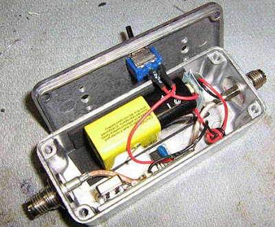
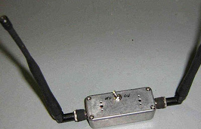
RF amplifier is doing its job perfectly yet (as it was mentioned in the Jammer Store blog post) draws additional power.Old aluminium box was used as a frame for the jammer and old UHF connectors from Motorola cell phone as input/output.You need to attach RF connectors to the circuit. Nine volt battery and voltage regulator were used to supply all components. The battery was placed inside and separated by the foamed plastic from the other components.The power on/off switch is placed on the top. The input and output antennas (also from old Motorola mobile phone) are screwed onto UHF connectors.Your cell phone jammer is ready. Enjoy!
Thursday, December 26, 2013
Build a Switch Mode Power Supply
The SMPS described here is suit-able for high-wattage stereos and other similar equipment. The circuit employs two high-voltage power transistors (BU208D) which have built-in re-verse-connected di-odes across their collectors and emitters. It can supply about 250-watt out-put. The circuit uses a ferrite core transformer of 14mm width, 20mm height, and 42mm length of E-E cores. An air gap of 0.5 mm is required between E-E junction. Good insulation using plastic-insulating sheets (Mylar) is to be maintained between each layer of winding.
Switch Mode Power Supply Circuit Diagram

The number of primary turns required is 90 with 26 SWG wire. The secondary winding employs 17 SWG wire (for 4A load current). Each turn of the secondary develops approximately 2 volts. The reader can decide about the output volt-age and the corresponding secondary turns, which would work out to be half the desired secondary voltage. The volt-age rating of capacitors C7 and C8 should be at least twice the secondary output of each secondary section. BY396 rectifier diodes shown on the secondary side can be used for a maximum load current of 3 amperes.
Two feedback windings (L1 and L2) using two turns each of 19 SWG wire are wound on the same core. These windings are connected to transistors T1 and T2 with a phase difference of 180o, as shown by the polarity dots in the figure. First wind the primary winding (90 turns using 26 SWG wire) on the former. Then wind the two feedback windings over the secondary (output). Ensure that each winding is separated by an insulation layer. Two separate heat sinks are to be pro-vided for the two transistors (BU208D).
The filter capacitor for mains should be of at least 47µF, 350V rating. It is better to use a 100µF, 350V capacitor. If the output is short-circuited by less than 8-ohm load, the SMPS would automatically turn off because of the absence of base current. The hfe min (current amplification factor) of BU208D is 2.5. Thus, sufficien base current is required for fully satu rated operation, otherwise the transistors get over-heated. At times, due to use of very high value of capacitors C7 and C8 (say 2200mF or so) on the secondary side or due to low load, the oscillations may cease on the primary side. This can be rectified by increasing the value of capacitor C6 to 0.01mF.
Author : Deepu P.A
Tuesday, December 24, 2013
Build A Homemade Fence Charger Energizer Circuit Explained
The electric fence charger circuit presented here is basically a high voltage pulse generator. The super high voltage is derived from a commonly used automobile ignition coil. An a stable multivibrator is used to generate the required frequency to drive the ignition coil. Another a stable is used to control the pulses supplied to the fence.
If you have large agricultural fields and desperately need to protect the crops from uninvited guests like animals and possibly humans, then this electric fence charger device is just what you are looking for. Build and install it yourself. An electric fence is an electrified high voltage barrier which produces painful shocks if physically touched or manipulated. Thus such fencing basically function as deterrents for animals as well as human intruders and stop them from crossing the restricted boundary.

The present circuit of an electric fence charger is designed and tested by me and has proved sufficiently powerful for the application. The circuit is able to produce voltage pulses up to 20,000 volts, needless to say about the fatality rate involved with it. However the pulses being intermittent, provides the subject with enough time to realize, recover and eject.
The generated pulse is so powerful that it can easily arc and fly-off between short distances of around a cm. so the fencing conductor needs to be separated adequately to avoid leakages through arcing and sparking. If not tackled, may drastically reduce the effectiveness of the unit.
Here the generation of high voltage is primarily carried out by an automobile ignition coil.
The winding ratios of an ignition coil are specifically designed and intended for creating high voltage arc between a two closely spaced conductors inside the ignition chamber to initiate the ignition process in vehicles.
Basically it’s just a step-up transformer, which is able to step-up an input applied voltage at its primary winding to monstrous levels at its output or the secondary winding.
SOME POINTS OF THE CIRCUIT AND THE IGNITION COIL IS VERY DANGEROUS TO TOUCH WHEN POWERED. ESPECIALLY THE IGNITION COIL OUTPUT IS TOO LETHAL AND MAY EVEN CAUSE PARALYSIS.
Let’s diagnose the whole thing more deeply.
Circuit Description
If you have large agricultural fields and desperately need to protect the crops from uninvited guests like animals and possibly humans, then this electric fence charger device is just what you are looking for. Build and install it yourself. An electric fence is an electrified high voltage barrier which produces painful shocks if physically touched or manipulated. Thus such fencing basically function as deterrents for animals as well as human intruders and stop them from crossing the restricted boundary.
The present circuit of an electric fence charger is designed and tested by me and has proved sufficiently powerful for the application. The circuit is able to produce voltage pulses up to 20,000 volts, needless to say about the fatality rate involved with it. However the pulses being intermittent, provides the subject with enough time to realize, recover and eject.
The generated pulse is so powerful that it can easily arc and fly-off between short distances of around a cm. so the fencing conductor needs to be separated adequately to avoid leakages through arcing and sparking. If not tackled, may drastically reduce the effectiveness of the unit.
Here the generation of high voltage is primarily carried out by an automobile ignition coil.
The winding ratios of an ignition coil are specifically designed and intended for creating high voltage arc between a two closely spaced conductors inside the ignition chamber to initiate the ignition process in vehicles.
Basically it’s just a step-up transformer, which is able to step-up an input applied voltage at its primary winding to monstrous levels at its output or the secondary winding.
SOME POINTS OF THE CIRCUIT AND THE IGNITION COIL IS VERY DANGEROUS TO TOUCH WHEN POWERED. ESPECIALLY THE IGNITION COIL OUTPUT IS TOO LETHAL AND MAY EVEN CAUSE PARALYSIS.
Let’s diagnose the whole thing more deeply.
Circuit Description
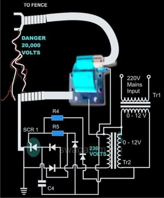
In the CIRCUIT DIAGRAMwe see that the entire circuit is basically comprised of four stages.
A DC oscillator stage, An intermediate 12 to 230 volts step-up stage, The voltage collector and firing stage and The super high voltage-booster stage.
TR1 and TR2 are two normal step-down transformers whose secondary windings are connected through SCR2. TR2’s input primary winding may be selected as per the country specification.
However, TR1’s primary should be rated at 230 volts.
IC1 along with the associated components forms a normal astable multivibrator stage. The supply voltage to the circuit is derived from the secondary of TR2 itself.
The output from the astable is used to trigger SCR2 and the whole system, at a particular fixed intermittent rate as per the settings of P1.
During the ON periods, SCR2 connects the 12 volt AC from TR2 to the secondary of TR1 so that a 230 volt potential instantly becomes available at the other end of TR1.
This voltage is fed to the voltage-firing stage consisting of the SCR1 as the main active component along with a few diodes, resistor and the capacitor C4.
The fired voltage from SCR1 is dumped into the primary winding of the ignition coil, where it is instantly pulled to a massive 20,000 volts at its secondary winding. This voltage may be suitably terminated into the fencing.
The high voltage generated by this electric fence charger will need to be carefully applied across the whole length of the fence.
The two poles from the ignition coil connected to the fence wiring should be kept at least 2 inches apart.
The pillars of the fence should be ideally made of plastic or similar non conducting material, never use metal and not even wood (wood tend to absorb moisture and may give path to leakages).
Parts List
R4 = 1K, 1WATT,
R5 = 100 OHMS, 1WATT,
P1 = 27K PRESET
C4 = 105/400V PPC,
ALL DIODES ARE 1N4007,
IC = 555
TR1 = 0-12V/3Amp (120 or 230V)
TR2 = 0-12V/1Amp (120 or 230V)
BOTH THE SCRs ARE C106 OR PREFERABLY BT151,
TWO WHEELER IGNITION COIL IS SHOWN IN FLUORESCENT BLUE COLOR
Sunday, December 22, 2013
Build an Alarm Control Keypad Circuit Diagram
The IC is a quad 2 input “AND” gate, a CMOS 4081. These gatesonly produce a HIGH output, when BOTH the inputs are HIGH. Whenthe key wired to `E` is pressed, current through R1 and D1switches Q5 on. The relay energises; and Q5 is `latched on` byR8. Thus, the Alarm is set by pressing a single key, say one ofthe tw1o non-numeric symbols.The alarm will switch off when the 4 keys connected to“A,B,C,D” are pushed in the right order. The circuit worksbecause each gate `Stands` upon its predecessor.If any key otherthan the correct key is pushed, then gate 1 is knocked out of thestack, and the code entry fails.
Pin 1 is held high by R4. This`Enables` gate 1; and when button `A` is pressed, theoutput at pin 3 will go high. This output does tw1o jobs.It locksitself `ON` through R2 and it `Enables` gate 2, by taking pin 5,high. Now, if `B` is pressed, the output of gate 2, at pin 4will go high. This output does tw1o jobs. It locks itself `ON`through R3 and it `Enables` gate 3 by taking pin 12 high.Now, if `C` is pressed, the output of gate 3 will lock itself`ON` through R5 and, by taking pin 8 high, `Enable` gate 4.Pressing `D` causes gate 4 to do the same thing; only this timeits output, at pin 10, turns Q4 `ON`.
This takes the base of Q5to ground, switching it off and letting the relay drop out. Thisswitches the alarm off.Any keys not connected to `A B C D E` are wired to the base ofQ1. Whenever `E` or one of these other keys is pressed, pin 1 istaken low and the circuit is reset. In addition, if `C` or `D`is pressed out of sequence, then Q2 or Q3 will take pin 1 low andthe circuit will reset. Thus nothing happens until `A` ispressed. Then if any key other than `B` is pressed, the circuitwill reset.Similarly, after `B`, if any key other than `C` is pressed,the circuit will reset. The same reasoning also applies to `D`.The Keypad needs to be the kind with a common terminal and aseparate connection to each key. On a 12 key pad, look for 13terminals. The matrix type with 7 terminals will NOT do.
Wire thecommon to R1 and your chosen code to `A B C D`. Wire `E` to thekey you want to use to switch the alarm on. All the rest go tothe base of Q1.The diagram should give you a rough guide to the layout of thecomponents, if you are using a strip board. The code you choosecan include the non-numeric symbols. In fact, you do not have touse a numeric keypad at all, or you could make your own keypad.I haven`t calculated the number of combinations of codesavailable, but it should be in excess of 10 000 with a 12 keypad; and, after all, any potential intruder will be ignorant ofthe circuit`s limitations. Of Course, if you must have a moresecure code, I can think of no reason why you shouldn`t addanother 4081 and continue the process of enabling subsequentgates. Or you could simply use a bigger keypad with more “WRONG”keys.Any small audio transistors should do.
The 27k resistors couldbe replaced with values up to 100k. And the only requirementsfor the 4k7 resistors is that they protect the junctions whileproviding enough current to turn the transistors fully on.Capacitors (C1 C2 C3 C4 C5) are there to slow response timeand overcome any contact bounce. They are probably unnecessary.
Alarm Control Keypad Circuit Diagram

Subscribe to:
Posts (Atom)
