Showing posts with label schematic. Show all posts

Monday, November 17, 2014

Timer 555 Schematic

Simple Timer With 555 is one example of a simple timer and can be applied to electronic equipment. With 555 Timer Simple series takes advantage of the mode of the IC monostable multivibrator 555. With the relay output control circuit can be used to control equipment with AC voltage source. With 555 Timer Simple circuit can work with source voltage of 5 - 12VDC depending on the relay used. In order to use Simple Timer With this 555 can be started by pressing the switch S1 to start the process of timing. In the relay there are 2 options that is normaly Close connection (NC) and normaly open (NO).
Timer

The duration of the timing circuit 555 Simple Timer With RC configuration is determined by the VR 1 MOhm and C 10uF. Active timer duration can be calculated with the formula T = 1.1 RC where T (seconds), R (Ohm) and C (farad). To get more accurate results R and C components referred to in the formula should use good quality components, namely C of tantalum material and R with the quality of 1%.
Here continue read..

Thursday, November 13, 2014

8 Watt Audio Power Amplifier Schematic

Here is the schematic for an 8 watt audio power amplifier. This amp can be used as a simple booster, the heart of a more complicated amplifier or used as a guitar amp. It is very small and portable unit and can be powered through 12V battery. I built the circuit on a Vero Board and had to add extra inductors, capacitors and resistors to prevent oscillation.

Circuit diagram:
 8 watt audio power amplifier schematic circuit diagram
8 Watt Audio Power Amplifier Circuit Diagram


Parts:R1 = 47K
R2 = 2.2R/1W
R3 = 220R/1W
R4 = 2.2R/1W
C1 = 100nF-63V
C2 = 10uF-25V
C3 = 470uF-25V
C4 = 2000uF-25V
C5 = 100nF-63V
IC1 = LM383
SPKR = 4ohm/8W

Notes:
  • IC1 must be installed on a heat sink.
  • C1 is for filtering and to prevent oscillation and should not be omitted.
  • The circuit can be built on a Vero Board, universal solder board or PC board, the PC board is preferred.
  • The circuit draws about 880Ma at 12 V.
  • By swapping the values of R2 and R3; you can turn this amplifier into a guitar amp with no preamp required.
  • If you cant find 2000uF, then replace C4 with a 2200uF unit.
  • If you add a 0.2uF capacitor in series with a 1 ohm resistor to the output you can prevent oscillation of the circuit under certain conditions.
Here continue read..

Tuesday, November 4, 2014

USB Switch Schematic

Anyone experimenting or developing USB ported peripheral hardware soon be comes irritated by the need to disconnect and connect the plug  in order to reestablish communication with the PC. This process is necessary for example each time the peripheral equipment is reset or a new version of the firmware is installed. As well as tiresome it eventually leads to excessive contact wear in the USB connector. The answer is to build this electronic isolator which disconnects the peripheral device at the touch of a button. This is guaranteed to reduce any physical wear and tear and restore calm once again to the workplace.

USB Switch Schematic Circuit Image :
 USB

The circuit uses a quad analogue switch type 74HC4066. Two of the switches in the package are used to isolate the data path. The remaining two are used in a classic bistable flip-flop configuration which is normally built using transistors. A power MOSFET switches the power supply current to the USB device.  Capacitor C2 ensures that the flip flop always  powers-up in a defined state when plugged  into the USB socket (‘B’ in the diagram). The  peripheral device connected to USB socket ‘A’  will therefore always be ‘not connected’ until  pushbutton S2 is pressed. This flips the bistable, turning on both analogue gates in the data lines and switching the MOSFET on. The  PC now recognises the USB device. Pressing  S1 disconnects the device.

USB Switch Schematic Circuit Diagram :

USB

The circuit does not sequence the connections as a physical USB connector does; the power supply connection strips are slightly longer than the two inner data carrying strips to ensure the peripheral receives power before the data signals are connected. The electronic switch does not suffer from the same contact problems as the physical  connector so these measures are not required in the circuit. The  simple circuit can quite easily be constructed on a small  square of perforated strip-board.

The design uses the 74HC(T)4066 type analogue switch, these have  better characteristics compared to the standard 4066 device. The USB switch is suitable for both low-speed (1.5 MBit/ s) and full-speed (12 MBit/s) USB ports applications but the proper ties of the analogue switches and perf-board construction  will not support hi-speed (480 MBit/s) USB operation.

The IRFD9024 MOSFET can pass a current of  up to 500 mA to the peripheral device with-out any problem.

Source: www.ecircuitslab.com/2012/06/usb-switch-schematic-circuit.html
Here continue read..

Sunday, September 21, 2014

Stereo Tube Power Amplifier Schematic

Stereo

This is the schema diagram of stereo tube power amplifier. It applies 3 types of tube that are 2 6SF5 GT high-mu triodes, 1 5Y3 GT vacuum rectifier, and 2 6K6 power beam amplifiers. The Audio input can be from any two-channel line level device such as a television, CD player, or VCR. It is of the tube type, using only 5 tubes total with no more than about 45 Watts power consumption from the outlet.


Components List:
R1,R10,R13 = 2.2M Ohm Potensiometer
R2 = 470K Ohm
R3 = 1M Ohm
R4 = 220K Ohm
R5 = 330 Ohm 2W Resistor
R6 = 220K Ohm
R7 = 2.2M Ohm
R8 = 1M Ohm
R9 = 720 Ohm 20W Resistor
R11 = 33K Ohm
R12 = 22K Ohm
C1,C9 = 4nF 400V Capacitor
C2 = 50nF 600V Capacitor
C3 = 20uF/25V
C4 = 10nF 400V Capacitor
C5 = 200pF 400V Ceramic Disc Capacitor
C6,C7 = 15uF 450V Capacitor
C8 = 15uF 400V Capacitor
T1 = 117V Primary, 350VCT Secondary, 6.3V Secondary, 6.3V Secondary
T2 = 7600 Ohm Primary, 4 or 8 Ohm Secondary
SW1 = SPST Switch
SP1,SP2 = 12" or smaller, 4 or 8 ohm speakers
MISC = 5 tube sockets, 2 RCA jacks, PC board or chassis, wire, knobs, etc.

Stereo Tube Power Amplifier Circuit Notes:
  1. C8 is for radio interference suppression and may be omitted.
  2. The 6V6 GT tube may be substituted for the 6K6 to lower power requirements.
  3. The 5Y3 GT tube should be mounted in a vertical position and be well ventilated. The 6K6 and 6SF5 tubes can be mounted in any position.
  4. The power supply portion of this unit may be used for anything requiring 290-320v DC up to about 3 amperes.
  5. Controls should have an audio taper.
Circuit Source: http://english.cxem.net/amplifier/amplifier13.php
Here continue read..

Friday, September 12, 2014

USB Switch Schematic Circuit

Anyone experimenting or developing USB ported peripheral hardware soon be comes irritated by the need to disconnect and connect the plug  in order to reestablish communication with the PC. This process is necessary for example each time the peripheral equipment is reset or a new version of the firmware is installed. As well as tiresome it eventually leads to excessive contact wear in the USB connector. The answer is to build this electronic isolator which disconnects the peripheral device at the touch of a button. This is guaranteed to reduce any physical wear and tear and restore calm once again to the workplace. 

Circuit image :
 USB
USB Switch Schematic Circuit Image

The schema uses a quad analogue switch type 74HC4066. Two of the switches in the package are used to isolate the data path. The remaining two are used in a classic bistable flip-flop configuration which is normally built using transistors. A power MOSFET switches the power supply current to the USB device.  Capacitor C2 ensures that the flip flop always  powers-up in a defined state when plugged  into the USB socket (‘B’ in the diagram). 

The  peripheral device connected to USB socket ‘A’  will therefore always be ‘not connected’ until  pushbutton S2 is pressed. This flips the bistable, turning on both analogue gates in the data lines and switching the MOSFET on. The  PC now recognises the USB device. Pressing  S1 disconnects the device.
Circuit diagram :
USB
USB Switch Schematic Circuit Diagram

The schema does not sequence the connections as a physical USB connector does; the power supply connection strips are slightly longer than the two inner data carrying strips to ensure the peripheral receives power before the data signals are connected. The electronic switch does not suffer from the same contact problems as the physical  connector so these measures are not required in the schema. The  simple schema can quite easily be constructed on a small  square of perforated strip-board. 

The design uses the 74HC(T)4066 type analogue switch, these have  better characteristics compared to the standard 4066 device. The USB switch is suitable for both low-speed (1.5 MBit/ s) and full-speed (12 MBit/s) USB ports applications but the proper ties of the analogue switches and perf-board construction  will not support hi-speed (480 MBit/s) USB operation. 

The IRFD9024 MOSFET can pass a current of  up to 500 mA to the peripheral device with-out any problem.


Here continue read..

Tuesday, September 9, 2014

LM377 Power amplifier schematic

Various needs of the amplifiers are all different. Different places and use also requires a different power amplifier as well. For this time i gave a circuit schematic power amplifier based on LM377 ic that has similarities with the LM378 and LM1877. Power is smoothly small ouput is 2 X 2.5 Watt and the impedance 4 ohms. Use of this amplifier suitable for portable radio tuner that can be taken every where.
Schematic
Component description :

Resistor
R1___________________2K
R2___________________2K
R3___________________1M
R4___________________1M

Capacitor
C1___________________4.7uF 50V
C2___________________4.7uF 50V
C3___________________100n
C4___________________100n
C5___________________470uF 50V
C6___________________470uF 50V

IC
IC1__________________LM377 , LM378 , LM1877
Here continue read..

Sunday, September 7, 2014

Schematic Audio Amplifier with IC A211D TBA611

See this circuit below:


Datasheet IC A211D
Vcc                = 4,5-15 V
Pout               = 1 W
RL                 = 8 Ohm
Ft                   = 50-15 Khz
Icco               = 10 mA
Package         = TABS4-14
Manufactered = RFT

Here continue read..

Monday, September 1, 2014

20W amplifier schematic with mute

This is a series of audio amplifier using ic and equipped with a mute switch. This circuit using ic and has 20W output impedance 4 ohms. Scheme and a list of components can be seen below.
20W
Read more
Here continue read..

Tuesday, August 5, 2014

Build a Cell Phone Jammer Schematic Diagram

Build a Cell Phone Jammer Schematic Diagram
 
This cell phone jammer operates at GSM800 frequency since most mobile phones use it to operate. So the selected VCO is a sweeping oscillator, which is very effective but may be hard to construct for the beginners without nice RF-testing equipment.

As a noise source you can use 45MHz clock oscillator which is driving Local Oscillator port located on a mini-circuit mixer. There is also an impedance matching network for Local Oscillator signal to pass through it. It is used to equate impedances of the clock oscillator and the port of the mixer.

RF input (which is this port of the mixer) connected to the first 800MHz cell phone antenna, and the RF output is sent to the mini-circuit amplifier. This amplifier increases the output power for 15-16dbm. The amplified signal then sent to the second cell phone antenna.

Build a Cell Phone Jammer Schematic Diagram


 works
All cell phones which use GSM800 have their transmitted and received frequencies always separated by 45MHz. So when the mobile phone tries to call it is blocked by its own signal returning to it! Isn’t that cool? When the phone blabber annoys you – turn your jammer on and that wrongdoer will hear own voice in his or her cell phone.

Oh, by the way, you can also use this mobile signal jammer to block any cell-based tracking systems which use your GPS to track and record your car’s moves. And it is quite possible (though I didn’t actually tested it) to jam IEDs which detonated using cell phones.

Build a Cell Phone Jammer Schematic Diagram


The mixer used is designed to work up to 600MHz but in this case it works pretty well.

Build a Cell Phone Jammer Schematic Diagram
 
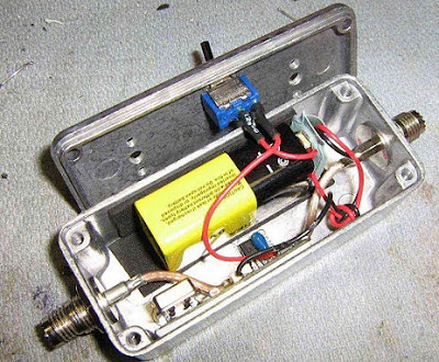
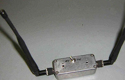
RF amplifier is doing its job perfectly yet (as it was mentioned in the Jammer Store blog post) draws additional power.Old aluminium box was used as a frame for the jammer and old UHF connectors from Motorola cell phone as input/output.You need to attach RF connectors to the circuit. Nine volt battery and voltage regulator were used to supply all components. The battery was placed inside and separated by the foamed plastic from the other components.The power on/off switch is placed on the top. The input and output antennas (also from old Motorola mobile phone) are screwed onto UHF connectors.Your cell phone jammer is ready. Enjoy!

Build a Cell Phone Jammer Schematic Diagram


Here continue read..