Friday, August 29, 2014

TV Remote Control Jammer


This is really fantastic schema.Because you can fun with this schema.If others operate your TV set or setup you can use this to control them.and you can use this to annoy someone.so enjoy with this....


Parts:

Q1 2N4403 PNP Transistor

Q2 2N4401 NPN Transistor

C1 10nF Ceramic Disc Capacitor

C2 1uF Electrolytic Capacitor

D1, D2, D3 High Output IR LED

R1 100K 1/4W Resistor

R2 150K 1/4W Resistor

R3 10K 1/4W Resistor

R4 1K 1/4W Resistor

S1 Normally Open Momentary Push Botton

B1 4.5V Battery (Three "AA"s In Series)

MISC Wire, Case, Board


Note

# You may need to adjust the value of R5 for the right frequency.
#supply 4.5v
Here continue read..

Thursday, August 28, 2014

Battery Saver Wiring diagram Schematic

A small electronic switch that connects a battery to the equipment for a certain amount of time when a push-button is momentarily pressed. And we have also taken the ambient light level into account; when it is dark you won’t be able to read the display so it is only logical to turn the switch off, even if the time delay hasn’t passed yet. The schema is quite straightforward. For the actual switch we’re using a well-known MOSFET, the BS170. A MOSFET (T2 in the schema) used in this configuration doesn’t need a current to make it conduct (just a voltage), which makes the schema very efficient. When the battery is connected to the battery saver schema for the first time, capacitor C2 provides the gate of the MOSFET with a positive voltage, which causes T2 to conduct and hence connect the load (on the 9 V output) to the battery (BT1). C2 is slowly charged up via R3 (i.e. the voltage across C2 increases).

Circuit diagram:


battery-saver-schema-diagramw
Battery Saver Circuit Diagram

This causes the voltage at the gate to drop and eventually it becomes so low that T2 can no longer conduct, removing the supply voltage to the load. In this state the battery saver schema draws a very small current of about 1 µA. If you now press S1, C2 will discharge and the schema returns to its initial state, with a new turn-off delay. Resistor R5 is used to limit the discharge current through the switch to an acceptable level. You only need to hold down the switch for a few hundredths of a second to fully discharge C2. In our prototype, connected between a 9 V battery and a load that drew about 5 mA, the output voltage started to drop after about 26 minutes. After 30 minutes the voltage had dropped to 2.4 V. You should use a good quality capacitor for C2 (one that has a very low leakage current), otherwise you could have to wait a very long time before the switch turns off! 

The ambient light level is detected using an LDR (R1). An LDR is a type of light sensor that reduces in resistance when the light level increases. We recommend that you use an FW150, obtainable from e.g. Conrad as part number 183547-89. When there is too little light its resistance increases and potential divider R1/R2 causes transistor T1 to conduct. T1 then charges up C2 very quickly through R4, which limits the current to a safe level. This stops T2 from conducting and the load is turned off. The choice of value for R2 determines how dark it has to be before T1 starts to conduct. The battery saver schema can be added to devices that use 6 or 9 volt batteries and which don’t draw more than 100 mA. The schema can be built on a piece of experimenter’s board and should be made as compact as possible so that it can be built into the battery powered device.


Copyright : Elektor Electronics
Here continue read..

2 x 75 W Audio Power Amplifier TDA7575

Features:

  • DMOS POWER OUTPUT
  • NON-SWITCHING HI-EFFICIENCY
  • SINGLE-CHANNEL 1Ω DRIVING CAPABILITY
  • HIGH OUTPUT POWER CAPABILITY 2x28W/
  • 4Ω @ 14.4V, 1KHZ, 10% THD, 2x40W/4Ω EIAJ
  • MAX. OUTPUT POWER 2x75W/2Ω, 1x150W/1Ω
  • SINGLE-CHANNEL 1Ω DRIVING CAPABILITY
  • 84W UNDISTORTED POWER
  • FULL I2C BUS DRIVING WITH 4 ADDRESS
  • ST-BY, PLAY/MUTE, GAIN 12/26dB, FULL
  • DIGITAL DIAGNOSTIC
  • POSSIBILITY TO DISABLE THE I2C
  • DIFFERENTAL INPUTS
  • FULL FAULT PROTECTION
  • DC OFFSET DETECTION
  • TWO INDEPENDENT SHORT CIRCUIT 
  • CLIPPING DETECTOR PIN WITH SELECTABLE THRESHOLD (2%/10%)
  • ST-BY/MUTE PINS
Block Diagram:
Block Diagram

Here continue read..

1959 Chevrolet Passenger Wiring Diagram

1959 Chevrolet Passenger Wiring Diagram
The part of 1959 Chevrolet Passenger Wiring Diagram: license lamp, backup lamp, dimmer switch, starter solenoid, spark plugs & distributor, clock lamp, cigarette lighter, neutral safety & backup switch.
Here continue read..

Wednesday, August 27, 2014

Voltage Monitor Wiring diagram Schematic

This is a very simple schema which can be modified to the users needs. Its operation is simple, when the input voltage is 0, the LED (LO). The LED turns off when the voltage increases to the level determined by R2.


Voltage Monitor Circuit Diagram

Voltage

Here continue read..

Wednesday, August 13, 2014

PCB Exposure Switch Timer V2 0

After some modifications on my UV exposure box (scanner) for better UV expose, i decided that a better pcb must me designed for switch timer. The old one had over drilled holes and it was designed and built on my very fist steps. Also the high voltage side from the low voltage wasn’t separated as it needed to be safe.
PCB Exposure Switch Timer V2.0

So i redesigned it in a more compact and easier to use pcb. The firmware has been also updated and now you can program the timmer by using the two buttons. The time is calculated by timer interrupt triggering using a 32.768KHz RTC Crystal with better accuracy. The display update also has been changed from static to dynamic. [Link]
Here continue read..

Tuesday, August 5, 2014

Build a Cell Phone Jammer Schematic Diagram

Build a Cell Phone Jammer Schematic Diagram
 
This cell phone jammer operates at GSM800 frequency since most mobile phones use it to operate. So the selected VCO is a sweeping oscillator, which is very effective but may be hard to construct for the beginners without nice RF-testing equipment.

As a noise source you can use 45MHz clock oscillator which is driving Local Oscillator port located on a mini-circuit mixer. There is also an impedance matching network for Local Oscillator signal to pass through it. It is used to equate impedances of the clock oscillator and the port of the mixer.

RF input (which is this port of the mixer) connected to the first 800MHz cell phone antenna, and the RF output is sent to the mini-circuit amplifier. This amplifier increases the output power for 15-16dbm. The amplified signal then sent to the second cell phone antenna.

Build a Cell Phone Jammer Schematic Diagram


 works
All cell phones which use GSM800 have their transmitted and received frequencies always separated by 45MHz. So when the mobile phone tries to call it is blocked by its own signal returning to it! Isn’t that cool? When the phone blabber annoys you – turn your jammer on and that wrongdoer will hear own voice in his or her cell phone.

Oh, by the way, you can also use this mobile signal jammer to block any cell-based tracking systems which use your GPS to track and record your car’s moves. And it is quite possible (though I didn’t actually tested it) to jam IEDs which detonated using cell phones.

Build a Cell Phone Jammer Schematic Diagram


The mixer used is designed to work up to 600MHz but in this case it works pretty well.

Build a Cell Phone Jammer Schematic Diagram
 
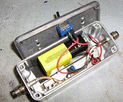
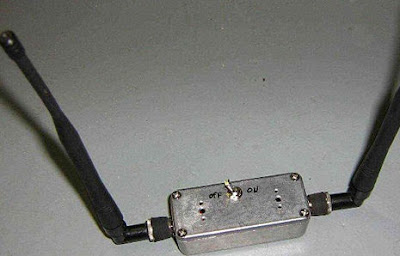
RF amplifier is doing its job perfectly yet (as it was mentioned in the Jammer Store blog post) draws additional power.Old aluminium box was used as a frame for the jammer and old UHF connectors from Motorola cell phone as input/output.You need to attach RF connectors to the circuit. Nine volt battery and voltage regulator were used to supply all components. The battery was placed inside and separated by the foamed plastic from the other components.The power on/off switch is placed on the top. The input and output antennas (also from old Motorola mobile phone) are screwed onto UHF connectors.Your cell phone jammer is ready. Enjoy!

Build a Cell Phone Jammer Schematic Diagram


Here continue read..