Thursday, November 20, 2014

Ultra Fast Battery charger circuit

Ultra Fast Battery Chager for Nickel-Cadmium battery cells [NiCad] which will be discussed in this article is Fast NiCad Battery Charger, called the Ultra Fast Charger Battery Charger NiCad because it can make filling fast NiCad Batteries Cell. A battery charger in Desai has a fast charging capabilities such as Ultra Fast Battery Chager for Nickel-Cadmium battery cells [NiCad] on this article shall be equipped with some ability to protect the battery and charger circuit itself.

Feature owned by Ultra Fast Battery Chager for Nickel-Cadmium battery cells [NiCad] 

  • Autoshut-off, is the ability of the charger to stop charging current to a NiCad battery if the capacity NiCad battery is fully charged.
  • Polarity Protection, with the existence of this capability so if there are mounting the battery on the charger upside yan can be known.
  • Constant output voltage
  • Output currents enough to fill some NiCad batteries at once in parallel.
  • Short Circuit Protection, with the existence of this protection circuit so if there is short-circuit caused by a battery and a charger circuit itself will not damage the other parts are not damaged.
  • Series Ultra Fast Battery Chager for Nickel-Cadmium battery cells [NiCad]


Image series above is a series of schematic drawings for Ultra Fast Battery Chager for Nickel-Cadmium battery cells [NiCad]. Ultra Fast Battery Chager for Nickel-Cadmium battery cells [NiCad] can be used for 8 to 10 NiCad batteries at once with 12 volt output voltage and max current is 3.5 A. The main components in the circuit of Ultra Fast Battery Chager for Nickel-Cadmium battery cells [NiCad] is UC3843 and MC34181. UC3843 chip is a voltage regulator and M34181 is a JFET OpAmp with characteristic low offset voltage, input impedance is very high. MC34181 serves as a voltage comparator.
Here continue read..

AT89Sxx Base Board

The board is based on the AT89S51, AT89S52, or AT89S53. This board uses STK200 for program loading and includes the serial port at the STK200 header. When I need to program the MCU and need a serial comunication, I do not need to plug and unplug the connector. Because I am using the USB to Serial ISP programmer. Then with the STK200, we must built the parallel programmer STK200. This parallel programmer STK200 can also be use for AVR programmer. This is the reason for the new design.
STK200
The PCB layout.
Here continue read..

Easy Downloader Circuit

Atmel microcontroller series AT89Cxx51 Easy Downloader is one of the downloader that is often used to write data to program the Atmel microcontroller AT89CXX51. Easy Downloader AT89Cxx51 ATMEL microcontroller is using the serial port as a channel of communication with the computer. Easy Downloader ATMEL Microcontroller AT89Cxx51 can be used to program Atmel AT89CXX51 in parallel. Atmel microcontroller series AT89Cxx51 Easy Downloader is quite simple to make your own because the components necessary to membutanya not complex. Atmel microcontroller series AT89Cxx51 Easy Downloader do not support the serial programming microcontrollers ISP. In the article Easy Downloader ATMEL Microcontroller AT89Cxx51 only displays images Easy Downloader Microcontroller series from Atmel AT89Cxx51 mengulasnya only and are simple.


Here continue read..

Wednesday, November 19, 2014

144 MHz Simple RF Detector Circuit


This simple circuit helps you sniff out RF radiation from your transmitter, improper joints, a broken wire or poor equipment with RF shielding. The tester is designed for the radio band amateur 2 meter (144-146 MHz in Europe). The instrument has a reading of 4-step LED and an audible alarm for high voltage radiation. The RF signal is received by an antenna and made to resonate by C1-L1. After rectification by the diode D1, the signal is fed to a two transistor Darlington amplifier HighGain, T2-T3. Assuming a 10-inch telescoping antenna using the RF level scale established for the LEDs is as follows:

When all the LEDs light, the (optional) UM66 sound / melody generator chip (IC1) also operates and provides an audible alarm. By changing the zener diode values ​​of D2, D4, D6 and D8, the step size and duration of the instrument may change as needed. To operate in other bands of ham or PMR, simply change the network-L1 C1 resonance.

For example, a transceiver 5 watt handheld equipped with a telescoping half-wave antenna (G = 3.5 dBd), there is an ERP (Effective Radiated Power) of just 10 watts and an emf of more than 8 volts near the head. Inductor L1 consists of 2.5 turns of 20 SWG (approximately 1 mm in diameter) enameled copper wire. The inner diameter is approximately 7 mm and no core is used.

Trimmer capacitor C1 associates is adjusted for the greatest number of LEDs to light at a relatively low fieldstrength position for a 2 m transceiver 145 MHz transmission. The tester is powered by a 9 V battery and consumes about 15 mA when all LEDs are on. Must be enclosed in a metal box.
Here continue read..

Preamplifier Microphone with 2 Transistor

Microphone preamplifier or often known as mic preamp can be made use simplemicrophone preamplifier circuit as follows. 2 microphone preamplifier circuit uses 2transistors are PNP and NPN transitor amplifier.

Front of the microphone amplifier orpreamplifier microphone 2 transistor uses a system of dc negative feedback through R6which serves to provide stability strengthening. Level output signal from the microphonepreamplifier is controlled by potentiometer P1. Input signal that can be responded well by this microphone preamplifier is 0.2 - 200mV and 1V RMS output will result.


   Component List      P1 2k2
     R1, R2, R3 100K 1/4W
     R4 8K2 1/4W
     R5 68R 1/4W
     R6 6K8 1/4W
     R7, R8 1K 1/4W
     R9 150R 1/4W
     C1 1uF 63V
     C2, C3, C4 100uF 25V
     C5 22uF 25V
     Q1 BC560C
     Q2 BC550C
 
Microphone preamplifier circuit two transistors in the show above is preampmic suitable for home audio system on the stereo. This microphone preamplifier circuit requires supply voltages 9Vdc.  
Here continue read..

TA8210AH Stereo Car Power Amplifier

IC TA8210AH By using this you can apply a series of audio power amplifier is the car audio system. In general, all the speakers in the car using a subwoofer speaker, and woofer. Because the car is not big room so the sound is being required is not too high.

Audio amplifier circuit can work at a minimum voltage 12-volt DC, if supplied under voltage 12-volt amplifier work will be less than the maximum. This amplifier output power up to 200W or 2 x 100W stereo with 8 ohm impedance.


Part List :

Resistor

R1 =1K
R2 =50K trim
R3 =1K
R4 =50K trim
R5 =680R
R6 =680R
R7 =150K
R8 =2R2
R9 =2R2
R10=2R2
R11=2R2


Capacitor

C1 =1uF
C2 =1uF
C3 =47uF
C4 =47uF
C5 =100n/400V
C6 =220uF
C7 =220uF
C8 =100n/400V
C9 =100n/400V
C10=100n/400V

Intregated Circuit

IC1=TA8210AH


Connector

X2-3=in R
X2-2=gnd
X2-1=in L
X1-1,X1-2=Out R
X1-3,X1-4=Out L
Here continue read..

Tuesday, November 18, 2014

230Volt LED Circuit
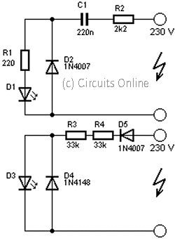
This is a circuit that is used to menhidupkan LED with voltage 230Volt, 230Volt it so that the voltage must be lowered in accordance with the needs of the LED itself. To lower it even necessary circuit as below.

230Volt

Here continue read..

Loop Control Automatic Reversing Circuit Diagram

LoopLoop Control Automatic Reversing Circuit Diagram

It is not the purpose of this folio to accommodate a abundant account of the ICs acclimated by this circuit. If you appetite added advice on this accountable amuse accredit to the Flip-Flop Made With A LM556 Timer Chip folio in the assorted circuits area of this armpit and additionally the Visible Light Photo Detector Circuits.

*The ambit uses the basal phototransistor detector ambit to faculty the position of a alternation that is abutting or is in the abandoning loop.

*Track polarity abandoning is not covered by this folio and will accept to be bent by the user.

Please Read Afore Using These Ambit Ideas

The explanations for the circuits on these pages cannot achievement to awning every bearings on every layout. For this acumen be able to do some experimenting to get the after-effects you want. This is abnormally accurate of circuits such as the "Across Track Infrared Detection" circuits and any added ambit that relies on added than absolute cyberbanking inputs, such as switches.

If you use any of these ambit ideas, ask your genitalia supplier for a archetype of the manufacturers abstracts bedding for any apparatus that you accept not acclimated before. These bedding accommodate a abundance of abstracts and ambit architecture advice that no cyberbanking or book commodity could access and will save time and conceivably accident to the apparatus themselves. These abstracts bedding can generally be begin on the web armpit of the accessory manufacturers.

Although the circuits are anatomic the pages are not meant to be abounding descriptions of anniversary ambit but rather as guides for adapting them for use by others. If you accept any questions or comments amuse accelerate them to the email abode on the Ambit Index page.

Here continue read..

Video Amplifier Circuits

Video amplifier circuit is simple and can be used. Video amplifier circuit was constructed from 2 pieces of transistors BC550 and BC560. The source voltage used for supplying the video amplifier circuit is 5VDC. Video amplifier circuit is equipped with a powerful regulator which flows through both transistors T1 and T2, the components used to manage these flows are P1 and P2. Then the video amplifier circuit is also equipped with limiting the maximum current that passes through T1 and T2. The components in black block functions as limiting the maximum current that is passed by the T1 and T2 for no more than 5mA.

Video

Here continue read..

Interface LCD SED 1200 and Mikorokontroler AT89C2051

Microcontroller AT89C2051 is a 20 pin version of the microcontroller AT89C51. Technical interface to microcontroller AT89C51 AT89C2051 and can be prepared very simply. SED 1200 LCD can be used to display 20 letters / numbers very good, quite adequate for displaying telephone numbers and other short message message. As the LCD display in general, SED1200 consists of two parts, namely the LCD panel which consist of many points LCD and a microcontroller attached to the panel and serves to set the dots LCDd be the letters / numbers that read, as well as functions for communication between the LCD display with another microcontroller using the LCD display. Task LCD display microcontroller users only send ASCII codes to be displayed.
Interface
In the data sheet says SED1200 LCD display is compatible with 4-bit microprocessor and 8 bits, this is due to SED1200 only equipped with 4 channels of data (DB0 .. db3) is used to distribute the ASCII code or command to set its SED1200. In terms of ASCII codes and commands are all 8-bit codes, the codes were sent twice, which first shipped is 4 bits are weighted higher (most significant bit - D4 .. D7) and then the remaining 4 bits (D0. . D3). In addition to DB0 .. db3, SED1200 also equipped with CS, WR and A0 such as components that are compatible with the microprocessor, which is somewhat distorted signal CLK lajut which will be discussed further below.

A0 is used to distinguish data that is sent to the SED1200, if A0 = 0 data sent is a command to control the SED1200 and vice versa if A0 = 1 data sent is ASCII code you want to display.

The process of sending data to the SED1200 depicted in Figure 1 can be described as follows:

CS signal is used to activate the process of sending this data, during this process CS activated by voltage level 0 .
The data will be sent to the SED1200 prepared at DB0 .. db3, as discussed above codes are sent to the SED1200 split into 2 time delivery, this is seen clearly in Figure 1 which describes the delivery of D4 .. D7 .. D0 and subsequent delivery D3.
After the data is ready, WR signal is used as a signal of commando for the SED1200 to retrieve the data on DB0 .. db3. Data collection is exactly what happened at the time of WR changed from 0 to 1
Interface to AT89C2051
AT89C51 AT89C2051 is a simplified into a microcontroller which only the legs of 20, a simplification that resulted AT89C2051 not have the legs DB0 .. DB7, P2.0 .. P27, WR, RD and ALE and how many other feet, other than that the instruction MOVX @ DPTR, A can not be used, thus the circuit of Figure 2 at all can not be used for the AT89C2051, and instead made the circuit of Figure 3, in this series and WR DB0 .. db3 replaced with Port 1 and its function is simulated through the program.

SED1200 CLK foot foot connected with P1.7 AT89C2051, SED1200 pulses required to process the received data generated by the program, it is not necessary to provide a special circuit to generate clock.

Cuts Program 2 is a sub-routine to control the SED1200 are connected to the AT89C2051 as shown in Figure 3, before taking the second sub-routine, the data to be sent to the SED1200 had to be prepared in the accumulator A.

Differences sub-routine and KirimASCII KirimPerintah lies in the value A0 at the time of the sub-routine work. Sub-routine KirimPerintah work with A0 = 0 (line 7), AT89C2051 received data sent as a command to set the SED1200 SED1200 work. Sub-routine KirimASCII work with A0 = 1 (line 11), received the data sent AT89C2051 SED1200 as ASCII code to be displayed
Throughout the process activated by the CS data transmission voltage level 0 is done in line 13 and in his re-nonaktip on line 19.
Data in the accumulator A is sent byte-by-half-byte half twice, first sent A4 .. A7 (lines 15 and 16) then sent A0 .. A3 (lines 17 and 18).
Given AT89C2051 no ALE signal instead row 22 to be raised 16 to 25 clock pulses required by the CLK SED1200. 16 pulse is generated after A.0 .. A.3 sent to the SED1200, out of the sub-routine is SED1200 is ready to receive data again.
Line 29 to 36 Discount Program 2 simulates line 21 Discount Program 1, in line 29 feet WR SED1200 in zero out, lines 30 to 35 send to DB0 A0 .. A3 .. db3 (P1.0 .. P1.3) without changing the other signals are already in Port 1. In line 36 WR returned to 1 , then that information on DB0 .. db3 taken by SED1200.
Here continue read..

Monday, November 17, 2014

DC Motor Speed Control using PWM

DC Motor Speed Control using PWM

The so-called PWM or Witdh modulation is a technique often used to control a load, for example, is the control of DC motor speed PWM techniques are used frequently.

Usually to make a simple PWM (for practice or the introduction PWM) fans to use some of the facts of the op-amp circuit, which consists of Schmitt Trigger circuit, the integrator and comparator.


Schmitt Trigger function that produces a square wave will become the sawtooth wave or integrator is also called common rail and the ramp compared to a reference voltage that can change a lot of stress. So the result is a PWM output.


These two schemes are variations of different circuit PWM. The diagrams are for 12V operation and there are upper (ground) and low side (+12 V common) versions. The version of the lower circuit uses an N-channel FET, the high-side version of the circuit uses a P-channel FET. N channel devices tend to handle more current P-channel devices, which are also less expensive. The version of the high side of the circuit is useful when a portion of the load must be grounded.

This circuit can change a fairly high amount of current, a MOSFET IRFZ34N can handle over 35 Amps if connected to an adequate heat sink. Higher power FETs, such as IRF1010Z IRFZ48N or can be substituted if even larger currents are required. It is also possible to connect multiple FETs in parallel even more current capacity. Always use thermally conductive grease between the FET and the heat sink, and remember that the heatsink is under stress.

Inductive loads (motors) may require special care because it can generate large voltage spikes that can damage the MOSFET. Replacing a 1N4002 fast recovery diode can help absorb the recoil reverse voltage when driving an inductive load like a motor. If you use these circuits to experiment with electric vehicles, be sure to install a circuit breaker in series with the battery, the switch should be easy to reach by the driver. This is especially important given the fact that when non-MOSFETs, is often cut, leaving the engine running at full speed
Here continue read..

PWMMotor Driver

As the title "PWM DC Motor Driver with Forward / Reverse and Breaking" this series is a PWM DC motor controller that can control DC motors with clockwise rotation and counter-clockwise and is equipped with a braking system.

In a series DC motor control PWM DC Motor Driver with Forward / Reverse and Breaking use this system for SASL PWM DC motor rotation speed. Power driver in a series DC motor PWM DC Motor Driver with Forward / Reverse and Breaking uses mosfet IRF150. Then, to control the direction of rotation of DC motor in the circuit of PWM DC Motor Driver with Forward / Reverse and Breaking uses relays. Then the braking system on a series of PWM DC Motor Driver with Forward / Reverse and Breaking is done by a resistor that is connected to the motor using relays.


Fig circuit PWM DC Motor Driver with Forward / Reverse and Breaking

PWMMotor Driver

See image details a series of PWM DC Motor Driver with Forward / Reverse and Breaking above. DC motor speed is set to pulse through the input PWM PWM, Power driver uses and the protection mosfet IRF150 with D7 as dumping. Then to start and stop is controlled via the logic input lines provided on the start / stop circuit PWM DC Motor Driver. Line inputs are used to set the reverse direction of rotation of DC motor that is with merberikan logic 1 / 0 on the path. R19 in the circuit of PWM DC Motor Driver serves as an expense to do the braking puteran DC motor.
Here continue read..

GSM Cell Phone Jammer Circuit

GSMGSM Cell Phone Jammer Circuit

A admirable diy gsm jammer or cellular adaptable buzz jammer schematic diagram for use alone in GSM1900 with abundance from 1930 MHz to 1990 MHz. The GSM1900 cellular corpuscle buzz arrangement is fabricated use of by USA, Canada and best of the nations in South America.

This cellular buzz jammer isnt applicative for use in Europe, Center East, nor Asia. The GSM jammer ambit could block adaptable adaptable buzz signals which operates on GSM1900 band, additionally articular as DCS.
Here continue read..

Timer 555 Schematic

Simple Timer With 555 is one example of a simple timer and can be applied to electronic equipment. With 555 Timer Simple series takes advantage of the mode of the IC monostable multivibrator 555. With the relay output control circuit can be used to control equipment with AC voltage source. With 555 Timer Simple circuit can work with source voltage of 5 - 12VDC depending on the relay used. In order to use Simple Timer With this 555 can be started by pressing the switch S1 to start the process of timing. In the relay there are 2 options that is normaly Close connection (NC) and normaly open (NO).
Timer

The duration of the timing circuit 555 Simple Timer With RC configuration is determined by the VR 1 MOhm and C 10uF. Active timer duration can be calculated with the formula T = 1.1 RC where T (seconds), R (Ohm) and C (farad). To get more accurate results R and C components referred to in the formula should use good quality components, namely C of tantalum material and R with the quality of 1%.
Here continue read..

Sunday, November 16, 2014

Kawasaki ZRX1200 Radiator Fan Circuit Diagram

KawasakiKawasaki ZRX1200 Radiator Fan Circuit Diagram

To inspect and service the 2001 to 2006 Kawasaki ZRX1200 R/S radiator fan system, do the following:

* Remove fuel tank.
* Disconnect the 2 pin connector from radiator fan switch.
* Using an auxiliary wire, connect the radiator fan switch leads of the main harness side.
* Turn the ignition switch ON. If the fan rotates, inspect the fan switch. If the fan does not rotate, inspect: leads and connectors, main fuse, fan fuse, and fan motor.
 
1. Radiator Fan
2. Radiator Fan Switch
3. Junction Box
4. Fan Fuse 10A
5. Main Fuse 30A
6. Battery 12V14Ah
Here continue read..

Friday, November 14, 2014

INVERTER CIRCUIT 100 WATT

Inverter is a small circuit which will convert the direct current (DC) to alternating current (AC). The power of a battery is converted in to’ main voltages’ or AC power. This power can be used for electronic appliances like television, mobile phones, computer etc. the main function of the inverter is to convert DC to AC and step-up transformer is used to create main voltages from resulting AC.

Block Diagram of Inverter


In the block diagram battery supply is given to the MOSFET driver where it will convert DC to AC and the resulting AC is given to the step up transformer from the step up transformer we will the get the original voltage.

Main Components

CD4047 : CD4047 is a multi vibrator with very low power consumption designed by TEXAS INSTRUMENTS.it can operate in monostable multivibrator and also astable multivibrator.in the astable multivibrator mode it can operate in free running or gatable modes and also provides good astable frequency stability. It can generate 50% duty cycle which will create a pulse, which can be applied for inverter circuit. This is mainly used in frequency discriminators, timing circuits frequency divisions etc.

IRF540 : IRF540 is a N-channel enhanced mode silicon gate field effect transistor (MOSFET).they are mainly used in switching regulators, switching converters relay drivers etc. the reason for using them in the INVERTER circuit is the because it is a high switching transistor , can work in very low gate drive power and have high input impedance.

IRF540 Symbol


Circuit Diagram


Explanation

  • In the circuit diagram we can observe that 12V battery is connecter to the diode LED and also connected to the pin8 of the IC 4047 which is VCC or power supply pin and also to pin 4 and 5 which are astable and  complement astable of  the IC. Diode in the circuit will help not give any reverse current, LED will work as a indicator to the battery is working or not.
  • IC CD4047 will work in the astable multivibrator mode. To work it in astable multivibrator mode we need an external capacitor which should be connected between the pin1 and pin3. Pin2 is connected by the resistor and a variable resistor to change the change the output frequency of the IC. Remaining pins are grounded .The pins 10 and 11 are connected to the gate of the mosfets IRF540. The pin 10 and 11 are Q and ~Q from these pins the output frequencies is generated with 50% duty cycle.
  • The output frequency is connected to the mosfets through resistor which will help to prevent to the loading of the mosfets. The main AC current is generated by the two mosfets which will act as a two electronic switches. The battery current is made to flow upper half or positive half of the primary coil of transformer through Q1 this is done when the pin 10 becomes high and lower half or negative half is done by opposite current flow through the primary coil of transformer, this is done when pin 11 is high. By switching the two mosfets current is generated.
  • This AC is given to the step up transformer of the secondary coil from this coil only we will get the increased AC voltage , this AC voltage is so high; from step up transformer we will get the max voltage. Zenor diode will help avoid the reverse current.

NOTE : The generated AC is not equal to the normal AC mains or house hold current. You cannot use this voltage for pure electric appliances like heater, electric cooker etc. Because of the fast switching of mosfets heat is dissipated which will effect the efficiency, use heat sink to remove this problem.
Here continue read..

INTERFACING HEX KEYPAD TO 8051

This article is about interfacing a hex key pad to 8051 microcontroller. A clear knowledge on interfacing hex key pad to 8051 is  very essential  while designing embedded system projects which requires character or numeric input or both. For example projects like digital code lock, numeric calculator etc. Before going to the interfacing in detail, let’s have a look at the hex keypad.

Hex Keypad

Hex key pad is essentially a collection of 16 keys arranged in the form of a 4×4 matrix. Hex key pad usually have keys representing numerics 0 to 9 and characters A to F. The simplified diagram of a typical hex key pad is shown in the figure below.


The hex keypad has 8 communication lines namely R1, R2, R3, R4, C1, C2, C3 and C4.  R1 to R4 represents the four rows and C1 to C4 represents the four columns. When a particular key is pressed the corresponding row and column to which the terminals of the key are connected gets shorted. For example if key 1 is pressed row R1 and column C1 gets shorted and so on. The program identifies which key is pressed by a method known as column scanning. In this method a particular row is kept low (other rows are kept high) and the columns are checked for low. If a particular column is found low then that means that the key connected between that column and the corresponding row (the row that is kept low) is been pressed. For example if  row R1 is initially kept low and column C1 is found low during scanning, that means key 1 is pressed.

Circuit Diagram

The circuit diagram for demonstrating interfacing hex keypad to 8051 is shown below.Like previous 8051 projects, AT89S51 is the microcontroller used here. The circuit  will display the character/numeric pressed on a seven segment LED display. The circuit is very simple and it uses only two ports of the microcontroller, one for the hex keypad and the other for the seven segment LED display.


The hex keypad is interfaced to port 1 and seven segment LED display is interfaced to port 0 of the microcontroller. Resistors R1 to R8 limits the current through the corresponding segments of the LED display. Capacitors C1, C2 and crystal X1 completes the clock circuitry for the microcontroller. Capacitor C3, resistor R9 and push button switch S1 forms a debouncing reset mechanism.


Program

ORG 00H
MOV DPTR,#LUT // moves starting address of LUT to DPTR
MOV A,#11111111B // loads A with all 1s
MOV P0,#00000000B // initializes P0 as output port

BACK : MOV P1,#11111111B // loads P1 with all 1s
       CLR P1.0 // makes row 1 low
      JB P1.4,NEXT1 // checks whether column 1 is low and jumps to NEXT1 if not low
      MOV A,#0D // loads a with 0D if column is low (that means key 1 is pressed)
       ACALL DISPLAY // calls DISPLAY subroutine
NEXT1 : JB P1.5,NEXT2 // checks whether column 2 is low and so on...
         MOV A,#1D
         ACALL DISPLAY
NEXT2 : JB P1.6,NEXT3
        MOV A,#2D
        ACALL DISPLAY
NEXT3 : JB P1.7,NEXT4
        MOV A,#3D
        ACALL DISPLAY
NEXT4 : SETB P1.0
        CLR P1.1
        JB P1.4,NEXT5
        MOV A,#4D
        ACALL DISPLAY
NEXT5 : JB P1.5,NEXT6
        MOV A,#5D
        ACALL DISPLAY
NEXT6 : JB P1.6,NEXT7
        MOV A,#6D
        ACALL DISPLAY
NEXT7 : JB P1.7,NEXT8
        MOV A,#7D
        ACALL DISPLAY
NEXT8 : SETB P1.1
        CLR P1.2
        JB P1.4,NEXT9
        MOV A,#8D
        ACALL DISPLAY
NEXT9 : JB P1.5,NEXT10
        MOV A,#9D
        ACALL DISPLAY
NEXT10 : JB P1.6,NEXT11
         MOV A,#10D
         ACALL DISPLAY
NEXT11 : JB P1.7,NEXT12
         MOV A,#11D
         ACALL DISPLAY
NEXT12 : SETB P1.2
         CLR P1.3
         JB P1.4,NEXT13
         MOV A,#12D
         ACALL DISPLAY
NEXT13 : JB P1.5,NEXT14
         MOV A,#13D
         ACALL DISPLAY
NEXT14 : JB P1.6,NEXT15
         MOV A,#14D
         ACALL DISPLAY
NEXT15 : JB P1.7,BACK
         MOV A,#15D
         ACALL DISPLAY
         LJMP BACK

DISPLAY : MOVC A,@A+DPTR // gets digit drive pattern for the current key from LUT
          MOV P0,A // puts corresponding digit drive pattern into P0
          RET

LUT : DB 01100000B // Look up table starts here
      DB 11011010B
      DB 11110010B
      DB 11101110B
      DB 01100110B
      DB 10110110B
      DB 10111110B
      DB 00111110B
      DB 11100000B
      DB 11111110B
      DB 11110110B
      DB 10011100B
      DB 10011110B
      DB 11111100B
      DB 10001110B
      DB 01111010B
END

About the Program

Firstly the program initializes port 0 as an output port by writing all 0′s to it and port 1 as an input port by writing all 1′s to it. Then the program makes row 1 low by clearing P1.0 and scans the columns one by one for low using JB instruction.If column C1 is found low, that means 1 is pressed and accumulator is loaded by zero and DISPLAY subroutine is called. The display subroutine adds the content in A with the starting address of LUT stored in DPTR and loads A with the data to which the resultant address points (using instruction MOVC A,@A+DPTR). The present data in A will be the digit drive pattern for the current key press and this pattern is put to Port 0 for display. This way the program scans for each key one by one and puts it on the display if it is found to be pressed.

Important Points

  • The 5V DC power supply must be well regulated and filtered.
  • Column scanning is not the only method to identify the key press. You can use row scanning also. In row scanning a particular column is kept low (other columns are kept high) and the rows are tested for low using a suitable branching instruction. If a particular row is observed low then that means that the key connected between that row and the corresponding column (the column that is  kept low) is been pressed. For example if  column C1 is initially kept low and row R1  is observed low during scanning, that means key 1 is pressed.
  • A membrane type hex keypad was used during the testing. Push button switch type and dome switch type will also work. I haven’t checked other types.
  • The display used was a common cathode seven segment LED display with type number ELK5613A. This is just for information and any general purpose common cathode 7 segment LED display will work here.
Here continue read..

Flashback VCR Cat Feeder from MAKE Volume 03


One of the most iconic projects from the pages of MAKE is the VCR Cat Feeder from MAKE Volume 03 (2005). It’s depressing to think of all the discarded VCRs in the world, but author James Larsson gave us a creative and useful way to repurpose this hunk of outdated machinery. Cats are wonderfully independent creatures for the most part, so when you’re leaving on a weekend trip, this programmable cat feeder is the ticket for keeping your feline companion well fed. Basically, you hijack a motor from inside the VCR, slow down its rotation with a gearbox, add an auger system with attached food container, and use the VCR’s timer-recording system to dispense scheduled meals. Some things never get old, like watching people’s facial expressions when you say “VCR Cat Feeder.”
Check out the full project on Make: Projects, and also watch this clip of John Park demoing the feeder on Make: television:
Here continue read..

Thursday, November 13, 2014

Radio Wave Alarm 4093 CMOS IC

This very simple alarm circuit is sure to have the police beating a path to your door - however, it has the added advantage of alerting you to their presence even before their footsteps fall on the doormat.


The alarm circuit transmits on MW (Medium Wave) (this is the small problem with the police). IC1a, together with a sensor (try a 20cm x 20cm sheet of tin foil) oscillates at just over 1MHz. This is modulated by an audio frequency (a continuous beep) produced by 4093 CMOS IC1b. When a hand or a foot approaches the sensor, the frequency of the transmitter (CMOS IC1a) drops appreciably.

Suppose now that the alarm circuit transmits at 1MHz. Suppose also that your radio is tuned to a frequency just below this. The 1MHz transmission will therefore not be heard by the radio. But bring a hand or a foot near to the sensor, and the transmitters frequency will drop, and a beep will be heard from the radio.
Here continue read..

using LM741 Simple Electronic Bell Generator

Today I begs for to advise Simple Electronic Bell Generator , with Linear IC Op-Amp the number is highly popular be number LM741. By when press S1 as a result , will have sound signal bell come out and lead this signal goes to amplify talk at one time with power Amplifier Circuit The general. For Circuit the this friends must use Dual Power supply Source 9 Volt. Detail sizes are other friends has seen in the circuit , which not difficult yes.

Here continue read..